Laser direct molding to achieve low cost 3D integrated circuits
Laser Direct Molding (LDS) technology uses laser ablation and metallization to create electronic circuitry on injection molded plastic parts while providing mounting surfaces for surface mount components, ultimately enabling 3D-mid.
Laser direct structuring creates a three-dimensional molded interconnect (3D-mid) on an injection molded plastic component housing that ablates circuit traces along its contour along the contour of the housing (see Figure 1). ). In the process of processing, firstly, according to the design scheme, the circuit traces are ablated on the plastic component shell by laser, and then the laser ablated portion is metallized, so that an electronic circuit is formed on the casing. The component housing is made of a high temperature resistant thermoplastic material so that surface mount components can be mounted using standard reflow soldering processes. 3D-mid brings a very obvious design and manufacturing advantages: more compact parts, smaller products, lighter weight, shorter assembly time and higher product reliability, and it is expected to be in medical, automotive, industrial And in some emerging applications in the military/defense sector, reducing overall system costs.

Figure 1: Three-dimensional molded interconnect device (3D-mid) integrates injection molded component housing and electronic circuitry
Three-dimensional direct molding
The LDS process begins with an element that has been injection molded from a thermoplastic composite. In this thermoplastic material, an organometallic additive is mixed into its polymer array. In fact, this organometallic additive is a metal particle encapsulated with an organic coating that does not significantly alter the inherent properties of the thermoplastic material. Commonly used thermoplastic materials are liquid crystal polymer (LCP), high temperature resistant nylon (PA6/6T), polytitarate (PPA), polybutylene terephthalate (PBT), PBT/PET and polycarbonate/ ABS plastic, etc.
First, the injection molded thermoplastic component is fixed in a laser system for surface activation. Prior to surface activation, the laser system has been programmed by the designer to input the corresponding CAD data. This process is often referred to as “incubation,†which is a key part of making the best molded parts because an optimal laser mode of operation is chosen based on the layout of the electronics.
Circuit traces were ablated using a diode-pumped ytterbium-doped yttrium vanadate (Nd:YVO4) laser with a power of 16W. The laser's acousto-optic Q-switch ensures that it provides highly stable pulses (pulse-to-pulse stability better than 1.5%), which is critical for achieving uniform activation of components. The Nd:YVO4 laser source with a wavelength of 1064 nm provides a pulse repetition frequency of 20 to 100 kHz. The system also uses a high-speed scanner and an optical Z-axis for three-dimensional beam transmission. The laser system has a maximum scanning speed of 4.0 m/s, and the ablation circuit trace and the beam diameter of the pad are 65 μm.
For a specific etched material, the first pass will give a good indication of whether or not the laser parameters need to be adjusted or optimized. According to the width of the LDS molding grade currently available, the laser power setting range is 2.0~7.0W, the frequency setting range is 40~100kHz, and the etching speed setting range is 2.0~4.0m/s. Of course, for each of the above three parameters, there is a recommended setting for each material, but if the best etched surface is not obtained with the recommended parameters, these parameters can be appropriately adjusted.
When the laser contacts the surface of the injection molded component, the resulting surface activation can achieve two different effects. First, the laser energy breaks the organic coating of the organometallic particles, exposing the metal particles to the surface of the component. Second, the components are etched along the traces of the laser beam, creating a rough surface that is easy to metallize (see Figure 2). Depending on the type of material used in the component and the laser parameter setting (mainly the power setting), laser etching creates a very small channel (depth 10 μm) or a very small ridge on the component. In areas where laser etching is not performed, the surface of the organometallic is not affected. Next, the laser-activated portion of the component is metallized.
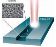
Figure 2: Laser Direct Forming (LDS) etches polymer materials to create an activated rough surface.
Easy to achieve metal plating
In selectConnect Technologies' patented selectConnect metallization process, the first step is electroless copper plating, which exposes the rough surface of the metal particles, creating a negative potential to deposit the copper layer. Due to the relatively poor oxidation resistance of copper, most 3D-mids were later selected for electroless nickel plating. Of course, it is also possible to deposit a gold layer that will provide superior oxidation resistance while providing an ideal mounting surface for surface mount components. For these metal coatings, typical coating thicknesses are: 100 to 600 microinches of copper (1 inch = 24.5); nickel is 50 to 100 microinches; gold is 3 to 8 microinches. Of course, depending on the actual application requirements, such as carrying a larger current, the coating of copper and nickel can be thicker. However, the thickness of the gold layer must be limited to 8 microinches because the process of plating the gold layer is not an autocatalytic process. If a thicker gold coating is required, the electroless gold layer is a viable option.
Application and restrictions
Currently, the most common application areas for LDS technology are wireless antennas and current-carrying circuits. LDS technology can be used to integrate a cell phone antenna into a functional plastic component inside the phone, eliminating the need for a separate metal antenna. In integrated mobile phone antenna applications, the benefits of LDS technology are realized: both component integration and product miniaturization, as well as component assembly work, are critical for high volume production and lower handset costs. In addition, LDS technology is easily combined with rapid prototyping to configure different antenna layouts. At present, many mobile phone antennas in the market are manufactured using LDS technology.
In addition to integrated mobile phone antenna applications, LDS technology is currently expanding into a wider range of applications. In essence, LDS technology integrates electronic circuits into mechanical plastic components. If there is no LDS technology, then at least a separate board or flexible circuit is required to carry the electronics.
Faced with packaging constraints, designers naturally challenge the limits of circuit layout. They want electronic circuits to become thinner and smaller, and the spacing between the two lines is getting smaller and smaller. Since the LDS technology uses a beam diameter of 65 μm, this is of course the theoretical minimum width, while in actual machining, the minimum width is at least twice the theoretical value. For the spacing between the two lines, the minimum spacing must be such that during the plating process, the two parallel electronic circuits do not intersect (short circuit). Based on practical experience to date, the minimum electronic line width suitable for production and the spacing between lines are 0.008 inches (8 mils) and 0.010 inches (10 mils), respectively. Of course, it is technically possible to achieve smaller circuit line widths and circuit spacings, but in actual processing it is necessary to carefully consider all aspects of the design to ensure a sufficiently reliable process for mass production.
As the flexibility of mounting surface mount components increases, it is now almost possible to use electronic circuit boards as part of mechanical plastic components (see Figure 3). For applications requiring lead-free reflow, the polymer LCP and PPA can withstand typical reflow temperatures; the polyamide PA6/6T resin supplied by BASF can withstand the necessary high temperatures. In plastic components, vias can also be created to connect the sides of the component, which gives the designer greater flexibility because the circuit can be placed on both sides of the component. Since the surface of the via needs to be laser activated, the design of the via can be achieved with a simple conical shape.

Figure 3: A circuit board for medical devices made with LDS technology,
Shows a unique integration of injection molded components with electronic circuitry and surface mount components
LDS technology has also opened up a wide range of applications in the medical field. In addition to the use of venulators, blood glucose meters, dental tools, hearing aids, pliers, temperature diagnostic pens and cleaning stations, a great example of LDS technology in medical applications is the DIAGNOdent diagnostic pen, which is used for A hand-held laser pointer for detecting caries lesions (decalcified or damaged areas of enamel, see Figure 4). The hand-held laser pointer was redesigned from a desktop instrument that uses 3D-mid components to achieve a significant reduction in size, weight and cost. An investment return study for the product showed that the use of LDS technology reduced the assembly time of the product from 20 seconds to 6 seconds, which greatly increased the assembly output, and also reduced the number of parts of the product from 8 to 3. The cost has achieved a huge reduction of 78%.

Figure 4: A handheld laser pointer made using LDS technology to detect caries lesions (decalcification of enamel or damaged areas in some way),
The appearance is small and light. Compared to traditional manufacturing methods, LDS technology has significantly reduced the total cost of the product by 78%.
In the automotive sector, we also see LDS technology in the field of steering hubs, brake sensors and positioning sensors. Applications for LDS technology in the industry include integrated Connectors, fully automatic samplers, motion sensors, and RFID antennas. In an automotive application, the detection of a rotating brake sensor in a high temperature, high humidity (85 ° C / 85% relative humidity) environment shows that after 1000 hours of testing, there are no 300 parts. defect. The material used in this application is the Vectra E840i (LCP). These test results once again demonstrate the stability and reliability of the LDS manufacturing process, which greatly encouraged the further expansion of LDS technology in automotive applications.
Shareconn development Co.,Ltd assemble series flat cables, we can accept small volume standard flat Cable Assemblies and customized Ribbon Cable Assemblies.
Our factory is qualified with ISO9001:2008, ISO13485:2003 and TS16949:2009 certificates, equipped with high-end automatic production equipment, like automatic crimping machines, automatic wire cutting and crimping machines, automatic crimping and tinned plate machines, etc. Meanwhile, we have our own laboratory to support the testing requirements from our suppliers and 100% checking before shipment. To assure the product and the comprehensive competence, we introduce high-level technical talents and management personnel as well as well-trained staff, and improve ourselves in many ways, like the quality, price, delivery, service, etc. Now, Shareconn has been the best supplier and partner for many customers.
Rainbow Flat Cable,Wire Rainbow Cable,Insulated Rainbow Flat Cable,Electronic Flat Ribbon Cable
Shareconn Development CO.,LTD , http://www.share-conn.com