Design and debugging of class D power amplifier circuit
A class D amplifier is a pulse signal that converts an input analog audio signal or PCM digital information into PWM or PDM, and then uses a PWM pulse signal to control a high power switching device to turn on/off the audio power amplifier. This article mainly introduces its design method.
1 system design
1.1 Overall design analysis
The system consists of high-efficiency power amplifier (class D audio power amplifier), signal conversion circuit, and external test instrument. The system block diagram is shown in Figure 1.
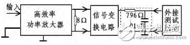
Figure 1 system block diagram
1.2 Design of Class D amplifier
The architecture of Class D amplifiers is symmetrical and asymmetrical. The Class D amplifiers discussed here are for portable applications that are very sensitive to power and volume. Therefore, a full-bridge symmetrical amplifier is used to make full use of its single Features of power supply and system miniaturization. The class D power amplifier consists of a PWM circuit, a switching power amplifier circuit and an output filter. The block diagram is shown in Figure 2.
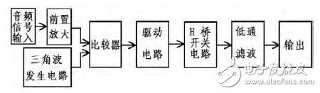
Figure 2D class audio power amplifier composition block diagram
A fixed-frequency PWM circuit consisting of a comparator and a triangular wave generator is used to modulate the triangular wave with the amplitude of the input audio signal, and a square wave whose duty cycle varies with the amplitude of the audio input signal is obtained, and the upper and lower bridges are driven in opposite phases. The power tube of the arm makes the power tube turn off when the power tube is turned on, and then converts the square wave into an audio signal through the output filter to push the speaker to sound. Balanced outputs are achieved with a full-bridge Class D amplifier, which improves the output filter characteristics of the amplifier and reduces interference. The peak-to-peak voltage of the full-bridge circuit load is close to twice the supply voltage and can be powered from a single supply. In the implementation, usually the two output pulse phase is opposite.
2 hardware circuit design
2.1 Principle analysis
The working process of the class D power amplifier is: when the analog audio signal is input, the analog audio signal is converted into a high frequency PWM pulse signal corresponding to the pulse width of the amplitude through the PWM modulator, and the switching unit is controlled to be turned on/off by the pulse pusher. The drive pulse power amplifier operates and then drives the speaker through a power low pass filter.
2.2 Comparator
The comparator circuit consists of a low-power, single-supply dual comparator chip LM311. In order to improve the system efficiency and reduce the unnecessary opening and closing of the CMOS tube in the rear H-bridge, the triangular waves with different biases are compared with the upper and lower halves of the audio signal respectively, and the potential at the positive end. When the potential is higher than the negative terminal, the comparator output is high, otherwise it is low. In this way, two mutually corresponding PWM wave signals are generated for processing by the subsequent stage driving circuit, and the two-way comparison circuit is as shown in FIG.

Figure 3 Comparator circuit
It is worth noting here that the upper half is processed as the audio signal connected to the negative end of the comparator, and the triangular wave signal is connected to the forward end; the lower half is compared to the opposite, so that they form a mutual correspondence and form a corresponding portion in the audio signal. When the PWM wave is used, the other half is low level, which can ensure that the CMOS tube in the rear H-bridge has no unnecessary opening and closing to reduce system power loss. The circuit uses the audio signal as the modulated wave, the triangular wave with the frequency of 70 kHz is the carrier wave, and the two signals are added with the DC bias voltage of 2.5V. The comparator compares to obtain the pulse with the same amplitude and the duty cycle varying with the audio amplitude. signal.
The power supply voltage of the LM311 chip is a single 5V power supply. To provide a static potential of 2.5V for V+=V-, take R10=R11, R8=R9, and take 4kΩ for all 4 resistors. Since the triangular wave Vp-p=2V, the Vp-p of the audio signal is required to be no more than 2V, otherwise the power amplifier will be distorted. Since the output stage of the comparator chip LM311 is an open collector structure, a pull-up resistor must be added to the output terminal, and the resistance of the pull-up resistor is a resistance of 1 kΩ.
2.3 drive circuit and complementary symmetrical output and low pass filter circuit
As shown in Figure 4. The PWM signal is shaped into a complementary symmetrical output drive signal, and the CD40106 Schmitt trigger is used in parallel to obtain a larger current output, and is sent to an output tube driven by a complementary symmetrical emitter follower composed of a transistor. A quick drive. The drive circuit transistor is a 9012 and 9014 pair of tubes.
The requirement of the H-bridge complementary symmetrical output circuit for the VMOSFET is that the on-resistance is small, the switching speed is fast, and the turn-on voltage is small. Because the output power is slightly larger than 1W, it is a small power output. It can be used with a relatively small power, a small input capacitance, and easy to drive quickly. The parameters of the IRF9630 and IRFZ48NVMOS pairs can meet the above requirements, so it is used. The actual circuit is shown in Figure 4. This design uses a 4th-order Butterworth low-pass filter.

Figure 4H bridge complementary symmetrical output and low pass filter circuit
The requirement for the filter is that the upper limit frequency is ≥ 20 kHz and the characteristics are substantially flat in the pass band. The complementary PWM switch drive signal alternately turns on Q6 and Q8 or Q12 and Q10, and is filtered by two 4th-order Butterworth filters to drive the horn.
3 circuit test
3.1 Debugging steps
1) Measurement of the passband: The amplifier voltage amplification factor is 10, and the upper and lower boundary frequency values ​​of the 3dB passband are measured. The RC filter for testing should be removed during passband testing.
2) Maximum undistorted output power: 10 times of amplification, input 1kHz sinusoidal signal, measure the effective value of amplifier output voltage with millivoltmeter, calculate the maximum output power Po-max. 3) Input impedance: A 10kΩ resistor is connected in the input loop, and the voltage drop at the input of the amplifier should be less than 50%.
4) Efficiency measurement: input 1 kHz sine wave, when the amplification factor is 10, make the output power reach 500mW, measure the power supply current I of the power amplifier (excluding the current for the test conversion circuit and the display part). The range of the power supply voltage V is required to be 5 & TImes; (1 + 1%) V. The efficiency is: 500mW%V&TImes;I.
3.2 Data Analysis
According to the above debugging steps, the measured data is shown in Table 1, Table 2, Table 3, Figure 5, and Figure 6.
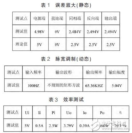

Figure 5 Error amplification (dynamic)
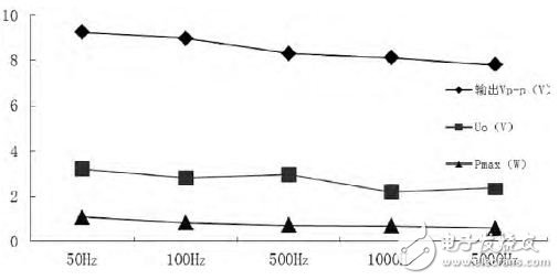
Figure 6 maximum undistorted power test data
Figure 5 shows the dynamic amplification error effect diagram when the amplitude of the input signal is unchanged and only its frequency is changed. As can be seen from the figure, for the signals outside the frequency band, the amplification factor and the output amplitude of the system are significantly reduced. For when the increase in signal frequency leads to EMI (electromagnetic interference) enhancement, low-pass filters can be used to reduce interference.
The power amplifier uses a 5V power supply, and the amplification factor of the preamplifier is adjusted to the maximum. The amplitude of the input signal is appropriately adjusted, the frequency is changed, and the maximum undistorted output power and efficiency are measured as shown in FIG. 6. For signals outside the band, the maximum undistorted power of the power amplifier is significantly reduced. To improve efficiency, the carrier frequency can be reduced, but the harmonic components and distortion of the output voltage increase. To reduce the nonlinear distortion of the output voltage, the frequency of the PWM modulated signal needs to be increased. Although high-frequency interference is a major problem in class D power amplifiers today, the advantages of high efficiency and energy saving have attracted more and more attention.
From the above data, there are some gaps between the efficiency of the power amplifier and the maximum undistorted output power and the theoretical value. The reasons are as follows:
1) There is static loss in the power amplifier circuit. The circuit has a certain power consumption under static conditions. The static total current of the 5V power supply is about 28mA. The static power consumption is: P loss=5&TImes; 28=140mW, the loss of this part has a great influence on the total efficiency. And the impact on the small power output is greater.
2) Loss of the output circuit of the power amplifier. This part of the loss has an effect on the efficiency and the maximum undistorted output power. The complementary excitation pulse of the H-bridge does not reach the ideal synchronization, and power loss is also generated.
3) The power loss of the filter, which is mainly caused by the DC resistance of the inductor, and the error of the power measurement circuit. In addition, there are measurement errors caused by the measuring instrument itself.
A new experience of true wireless
Automatic seconds connection, can be used with headphones
Professional sound engineering technology
Case Cube/acoustic clear sound reproduction
customized stainless steel acoustic structure, high quality grahene hoop system and obvious environmental noise attenuation will open up a pleasant journmey journey for you to enjoy the sound.
Built-in microphone/ Effective noise reduction/ Clear call/ Easy to carry
Sports can't be abandoned more freely
Close ergonomic design, close to the ear, even wearing for a long time can also enjoy comfortable experience.
And can form a triangular stable support with the ear, even if running and riding, vigorous fitness is still close to the ears, wildly shake off.
Bluetooth Earbuds,True Wireless Earbuds,Wireless In Ear Gaming Headset,Wireless Bluetooth Headphones
Guangzhou HangDeng Tech Co. Ltd , https://www.hangdengtech.com