Multi-core DSP multi-channel synchronous clock signal design analysis
Abstract: Multi-core digital signal processors (DSPs) have a rich set of peripheral interfaces, each with its own independent reference clock. Due to the fast data processing capability of multi-core DSPs, the clock requirements for peripheral interfaces are high. When multiple interfaces work together, the clock synchronization requirements are high. This paper introduces the clock design of multi-core digital signal processor Ding MS320C6678. The clock chip CDCM6208 provides multiple clock signals of different working frequencies to the DSP. The paper introduces the initialization and setting of the clock chip and the detailed software and hardware design methods.
introduction
Multi-core processors are recently evolving electronic devices. Multiple isomorphic or heterogeneous processors are integrated into a single chip, which greatly improves the computational processing power. DSP processors are widely used due to their high digital processing capabilities. The multi-core DSP chip takes the TMS320C66 series with higher performance as an example. The TMS320C6678 (hereinafter referred to as C6678) contains 8 processors. These processors can work independently or in parallel. When they work together, it is important to communicate and handshake with each other, especially in situations where time is high, clock stabilization and synchronization are critical. The stability and synchronization of the clock puts high demands on system design, clock source, clock distribution, circuit wiring, and clock line shielding.
This article uses the CDCM6208 clock distribution chip to output multiple clocks, and provides the 8-core DSP chip C6678, which provides clock signals such as DSP core working clock, DDR3 data read/write clock, RapidIO and PCIe data transmission clock, and Gigabit network accelerator. The paper introduces detailed circuit design, clock chip configuration, and configuration of multi-core DSP, and initialization of related on-chip devices.
1 C6678 and its structure
The C6678 is an 8-core floating-point DSP from TI's multi-core processor with a maximum operating frequency of 1.25 GHz. The single core can provide 40GMAC fixed-point calculation or 20G FLOP floating-point computing capability. A single chip can provide 320G MAC or 160G FLOP calculation. ability. The on-chip structure of the C6678 is shown in Figure 1.
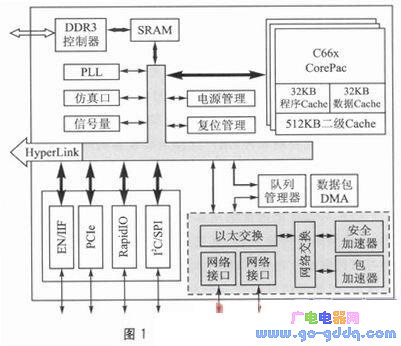
Each core of the C6678 has a 32 KB program, 32 KB of data, and 512 KB of Level 2 Cache memory. The chip has a 4 MB shared SRAM. The C6678 has a DDR3 controller interface that can be externally connected to DDR3 with a direct addressing range of 8 GB. The C6678 has RapidIO, PCIe, EMIF, and interfaces such as SPI and I2C bus. These interfaces interact with each processor through the on-chip high-speed interconnect bus.
The network-related on-chip devices are shown in the gray module in the lower right corner of Figure 1. They mainly include two external SGMII interfaces, Ethernet switching and network switching modules, and security accelerators and packet accelerators for data management, in order to quickly detect data. The verification and the protocol comply with the network standard, and directly discard the wrong data. Reduce the burden on the CPU. In order to speed up the data exchange between the network and the CPU, the on-chip queue manager is used to manage the function of buffering and distributing network packets or network frames. These data are read/written using packet DMA and do not require CPU involvement.
Other on-chip devices in the C6678 include PLLs, emulation ports, semaphores, power management, and reset management. The PLL configures the working clock of the CPU and peripherals; the emulation port is used to connect the emulator to realize the monitoring of the software operation; the semaphore realizes the control of the semaphore in the DSP/BIOS operating system; the power management realizes the control of the current and voltage of the whole chip. ; reset management
Set the startup mode, hard reset for full boot, soft reset for partial boot.
2 CDCM6208 and its structure
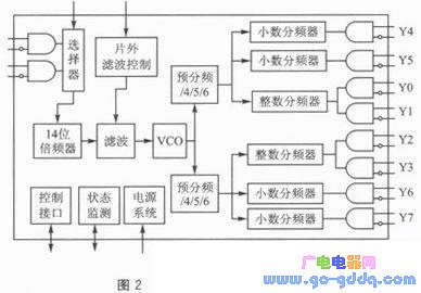
The CDCM62xx family of chips is a clock generation, driver and distribution chip developed by TI for multi-core processors. The CDCM6208 is the second generation of this series. Compared with the first generation CDCM6208, the biggest advantage is that the power consumption is greatly reduced, from 2 to 3 W in the first generation to about 0.5 W. Its function, indicator and volume are not weakened. The CDCM6208 has two optional clock inputs and eight clock outputs. The 4 channels of the 8 outputs can only be divided into integer multiples, and the other 4 channels can be divided by a fractional multiple to meet the various clock requirements of multi-core chips. The 8-channel clock supports LVPECL, CML, HCSL, and LVDS signal levels, and supports up to 800 MHz clock frequency to meet the high-speed interface requirements of RapidIO and PCIe. The clock jitter is less than 265 fs. Its control can be realized through standard SPI or I2S interface, which is very convenient and flexible. TI provides graphical control software specially developed for this chip, and the user selects the clock working method to be set.
The parameters such as the output frequency and the output frequency, the software generates the value of its internal register, and completes the configuration of the entire chip by writing through the SPI or I2S interface.
The internal structure of the CDCM6208 is shown in Figure 2. As can be seen from the figure, after two clock inputs are selected, a 14-fold multiplier is first used as a reference clock to drive the on-chip VCO to generate a clock signal. In order to improve the clock phase noise, the multiplied signal passes through an on-chip filter, which can be set by an on-chip RC circuit. The VCO clock is divided into two prescalers, and the prescaler can only be divided by 4, 5 or 6. After the prescaler, the clock enters the later divider again. Each prescaler is divided into two fractional dividers and one integer divider. After the frequency is divided, the signal is driven and output. As can be seen from the output on the right side of Figure 2, the Y0 and Y1 clock frequencies of the integer divider output are the same, and the Y2 and Y3 clock frequencies are the same. The fractional division of Y4~Y7 can set the clock configuration of CDCM6208 to limit its application, but the advantage is to reduce the power consumption. At present, this configuration meets the requirements of most multi-core processors, especially TI's C66 series. And the AK2 series of multi-core DSPs can be seamlessly connected.
3 hardware design
According to the application of TMS320C6678, the required clock is shown in Figure 3.
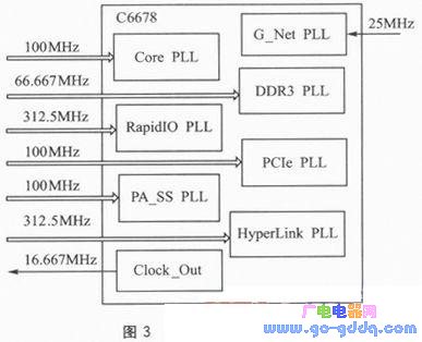
Its main clock consists of a 1-core running clock that is 100 MHz and the DSP on-chip PLL locks it to the operating frequency, up to 1 GHz and a minimum of 700 MHz. 2RapioIO interface and HyperLink super-connect interface working clock, both clock inputs are 312.5MHz, and RapioIO multipliers 4, 8, 10, 16 work at 1.25 GHz, 2.5GHz, 3.125 GHz and 5 GHz. HyperLink multiplies to 40, 80, 100, 160 and operates at 12.5 GHz, 25 GHz, 31.25 GHz, and 50 GHz.
3 PCIe interface clock and PA_SS network accelerator clock. Both clocks are input to 100MHz, and the corresponding working clock after internal multiplication meets the transmission clock requirements of the respective interfaces. 4DDR3 clock, this clock input is 66.667 MHz, multiplying 20 or 25 times, working at 1333.33 MHz or 1666.7 MHz. These clocks have independent PLL circuit settings in the DSP chip, and their working principle and setting method are basically the same. The separate 25 MHz in Figure 3 is the operating clock dedicated to the Gigabit network, provided by a single crystal. The C6678 also provides a clock output signal. The default output is 1/6 of the core clock. In the figure, it is 16.667 MHz. The output clock can detect whether the C6678 is working normally.
Portable energy storage power Stastion
SHENZHEN CHONDEKUAI TECHNOLOGY CO.LTD , https://www.szsiheyi.com