How about Samsung 10nm? Comparison of 10nm process and 14nm process
As we all know, in November 2016, Samsung has already begun to apply 10LPE manufacturing technology to its SOCs. Compared with the 14LPP process used by Samsung, this manufacturing technology will be able to reduce the chip area by 30%, while reducing power consumption by 40% or improving performance by 27% (with the same energy consumption). So far, Samsung has used this technology to process more than 70,000 wafers. From this process, Samsung's technology can be roughly estimated (considering the 10nm process production cycle is about 90 days).
At the same time, we should know that Samsung has not yet launched many 10nm process products: only Samsung's own Exynos series and Samsung's 835 chip OEM for Qualcomm use Samsung's 10nm process.
In addition to the above products, Samsung plans to mass-produce chips using the second-generation 10nm process by the end of 2017, which is what Samsung calls the 10LPP process. In the future, Samsung will launch a third-generation 10nm process chip (10LPU) at the end of 2018. Last year, Samsung said that the 10LPP process has improved performance by about 10% over the existing 10LPE process. Samsung Electronics announced its chip development plan not long ago. Samsung’s first-generation 10-nanometer FinFETLPE process was mass-produced in October last year. Of course, it is basically provided for Qualcomm S835 and Samsung Exynos8895. According to the current Samsung’s planned stocking volume, Its 10nm yield rate is only about 70%, far less than TSMC's yield rate of over 85%, but the progress of Snapdragon 835 and 8895 is much higher than that of MediaTek’s x30, which makes TSMC lag behind Samsung in name. However, Samsung's current daily production capacity has increased to about 25,000 pieces per month, which can provide about 3 million pieces of 10nm chips per month.
Comparison of 10nm process and 14nm process In the chip market, the specific value of a chip manufacturing process is a key indicator of mobile phone performance. Every improvement in process technology brings about performance enhancement and power consumption reduction. The release of each flagship mobile phone is often inseparable from the breakthrough of chip performance.
For example, the Snapdragon 835 of Xiaomi Mi 6 uses a more advanced 10nm process. With more than 3 billion transistors integrated, the volume is 35% smaller than the Snapdragon 820, and the overall power consumption is reduced by 40%. But it rose by 27%. In addition, the 10nm process technology increases the design and manufacturing cost by nearly 50% compared to the 14nm process. It is the only way for large manufacturers to continue and huge capital investment into the mass production of 10nm chips.
10nm and 14nm refer to the manufacturing process of the processor. The higher the level of technology, the lower the power consumption and the lower the heat generation under the same performance. Therefore, the processor also saves power. At the same time, the heat is reduced. In the case of the same temperature threshold, the processor can make the frequency higher, which results in higher performance and is conducive to long-term high-frequency operation. It is very helpful to reduce the occurrence of mobile phone heating and improve the comprehensive experience of mobile phones
The two core elements of the mobile phone chip upgrade are the architecture and the process. The architecture is the CPU core micro-architecture of the mobile phone chip, and the other element is the semiconductor manufacturing process. The Snapdragon 820 uses the 14nm FinFet process of Samsung Semiconductor and the Snapdragon 835. It adopts the latest 10nm process. The manufacturing process largely determines the power consumption level of a chip. The more advanced the process (the smaller the XXnm number), the lower the power consumption of a chip. The power consumption of Snapdragon 835 and Snapdragon 820 Compared with the size, the Snapdragon 835 with more advanced manufacturing process is significantly smaller. The power consumption of the Snapdragon 835 with the 10nm process is definitely lower than that of the Snapdragon 820 with the 14nm process
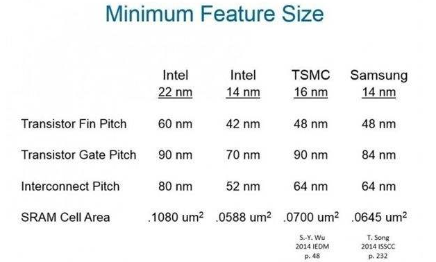
The SOC process is divided into 10nm, 14nm, 16nm, etc., which can be distinguished from the following aspects:
First, you need to figure out how big the nanometer is. For example, if you actually measure it with a ruler, you can know that the thickness of the nail is about 0.0001 meters (0.1 mm), that is, try to cut the side of a nail into 10 Ten thousand lines, each line is approximately equivalent to 1 nanometer, so you can slightly imagine how tiny 1 nanometer is.
Second, come back to explore what the nano process is. Taking 14 nanometers as an example, the process means that in the chip, the smallest wire can be as small as 14 nanometers. The main purpose of reducing transistors is to be in a smaller chip. Insert more transistors, so that the chip will not become larger due to technological advancement; secondly, it can increase the computing efficiency of the processor; secondly, reducing the size can also reduce power consumption; by reducing the length of the gate, the current can be Use a shorter path from Drain to Source.
Finally, after the size of the chip is reduced, it is easier to plug into mobile devices (such as mobile phones) to meet the future needs of thinner and lighter.
Crystal Clear Back Sticker,Phone Sticker,Mobile Phone Back Skin,Crystal Clear Phone Skin
Shenzhen Jianjiantong Technology Co., Ltd. , https://www.hydrogelprotectivefilm.com