In-vehicle application for high-speed video detection with MPC5200
Automakers are increasingly improving the safety of their cars by processing high-speed video images captured inside and outside the car. For example, a camera mounted in a car can be used to determine the position of the passenger within the vehicle to optimally configure the airbag and protect the passenger from injury. Cameras installed in different positions in the car can also be used for lane departure monitoring, pre-crash warnings, collision avoidance, rear reversing light warnings and distance calculation. Many of these applications require video images to be captured at very high rates. Accordingly, video images must be processed by sophisticated algorithms in real time to provide feedback to the safety control system within the vehicle. This is a very important task to avoid collisions or to determine the position of the passengers in the car at the moment the vehicle collides. Moreover, the technology requires that the engine-side insulation panel on the driver's side must withstand temperatures up to 85 °C, while other parts of the vehicle must withstand temperatures up to 105 °C.
This article refers to the address: http://
--- --- 
Currently, the challenge for automakers is to have a cost-effective technology: powerful processing power, rich interfaces, good environmental adaptability and low-power operation. The MPC5200 high-performance embedded processor from Freescale Semiconductor meets all of these design requirements and its structure is shown in Figure 1.
--- The MPC5200 integrates a high-performance MPC603e core that achieves 760 MIPS of processing power at 400 MHz operating frequency and temperature range of -40 to 85 °C. High-performance, double-precision floating-point unit (FPU) speeds up complex mathematical operations parallel to other mission-critical tasks. Models that operate at 105°C can also be used outside the driver's seat where higher temperature levels may be required .
--- With the help of the FPU, the MPC5200 processing capability provides sufficient support for most video detection algorithms. The integrated PCI interface provides a standardized high-speed interface for CMOS image sensors. The CMOS image sensor can transfer image data to the MPC5200 at 80 to 100 frames per second, depending on the PCI clock and photo resolution.
---BestComm intelligent DMA controller can speed up the transmission of camera data into memory for processing, thus minimizing the load on the core of MPC603e main processor, making it free to handle tasks such as video detection algorithms. In addition, the use of the BestComm controller can reduce the overall outage load on the primary core, which in turn accelerates overall throughput. The integrated CAN and J1850 controllers, combined with external MOST (media-oriented system transport) support, provide cost-effective integration for the rest of the automotive safety system and reduce the latency of communication with these networks.
--- The following describes how to design a basic high-speed camera interface circuit for the MPC5200 through the PCI interface. In this example, the Freescale MCM20014 CMOS sensor is used, but other sensors can use almost identical interface mechanisms. The interface is very straightforward and requires less interface logic to complete the connection.
Clock hypothesis using the MPC5200
--- The most likely XLB release target frequency is 132MHz; IPBus is 66MHz; PCIclk (external bus clock) is 66MHz; XTAL's expected input frequency is 33MHz. For this application, the maximum PCI frequency is 33MHz.
--- The clock ratio between XLB and IPBus, IPBus and PCIclk may be 4:1, 2:1 or 1:1. When the XLB is 132MHz, the IPBus must be set to 4:1 or 2:1 (for IPBus of 33MHz or 66MHz respectively). Depending on the IPBus (33MHz, 16.5MHz working with 33MHz IPBus; or 33MHz working with 66MHz IPBus), PCIclk may support a 1:1 ratio or a 2:1 ratio. On the processor side, a 66MHz PCIclk may be used, but the image sensor on the market has not yet reached this speed.
--- If a 50% duty cycle is required, the PWM output value that generates HCLK can only be an even integer quotient of the IPBus clock.
--- Here are a few possible clock relationships.
---XTAL: 27MHz, XLB: 108MHz, IPB: 54MHz, PCI: 27MHz, HCLK: 13.5MHz (4/1 ratio PWM from IPBus clock)
---XTAL: 33 MHz, XLB: 132MHz, IPB: 66MHz, PCI: 33MHz, HCLK: 8.25MHz (8/1 ratio PWM from IPBus clock)
The ---XTAL input can be varied to produce different operating frequencies, but the 8.25 MHz HCLK should be suitable for the camera, and it also provides a 4:1 difference between the DMA clock and the sensor data rate (PCIclk to HCLK). This helps with potential bandwidth issues that may occur.
--- The solution is to provide interface logic between the sensor data bus and the PCI data bus. The interface logic of the MPC5200 is very simple, but there are still some system application issues that must be carefully considered. One of the things to note is whether to use the PCI bus for purposes other than camera data transmission. If you need to share the PCI bus with other devices, the interface logic must coexist with other PCI targets, which requires additional circuitry. If you don't need to share the PCI bus with any other device, the interface logic can assume that any PCI processing is for it, so the logic becomes very simple.
--- Figure 2 is a connection diagram of the MPC5200 with the interface chip and CMOS sensor, showing the MPC520 PCI signal connected to the required interface logic or directly connected to the sensor. The thick line in Fig. 2 indicates the case of three states. The bus requires an external pull-up resistor so that the interface logic will have a logic number "1" in its input value.

--- The sensor is displayed during its frame valid period: one frame on the sensor is ready for transmission. The signal will be connected to the MPC5200 through the IRQ line. The frame transmission needs to be driven by the MPC5200 PCI controller. The signal timing is shown in Figure 3. The specific steps are as follows.
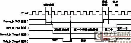
â— The MPC5200 PCI causes Frame_b to output a low level to begin processing. The AD line is driven by the MPC5200 via address information. Interface logic can ignore this phase.
â— The MPC5200 PCI causes Irdy_b to output a low level to initiate the data phase. The AD line is still pushed by the MPC5200 until the target (interface logic) determines that Devsel_b "requires" the process.
â— As long as the target keeps Trdy_b high, the MPC5200 PCI can put the AD bus in a tri-state and remain in a wait state.
â— At any edge of the PCIclk that just appeared, where Trdy_b is detected as low, PCI captures the data and considers it to transmit a data beat.
â— After completing the next to last data shot, the MPC5200 PCI causes Frame_b to output a low level, which indicates that the last data shot is being requested.
â— When the target transmits the last data beat (marked as Trdy_b goes low), the MPC5200 PCI causes Irdy_b to output a low level and the processing is completed.
• There are other signals related to PCI processing, but they are not required for this purpose in the case of PCI transmission errors.
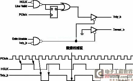
--- If the ratio of HCLK to PCIclk is 2:1, the connection of PCIclk to the interface logic is not necessary. If the ratio of PCIclk to HCLK is 4:1 (which is more desirable), a flip-flop is needed to delay and shorten the duration of the PCI signal Trdy_b.
--- When compatible with a 3.3 volt CMOS camera sensor tri-states its data bus, the sensor's data line is directly and efficiently connected to the PCI AD bus. Otherwise, a data repeater is needed in this design. When judging the LineValid signal of the sensor, the sensor should only drive the data line. Figure 4 is a 2:1 logic diagram of 27 MHz PCIclk versus 13.5 MHz (or similar frequency) HCLK.
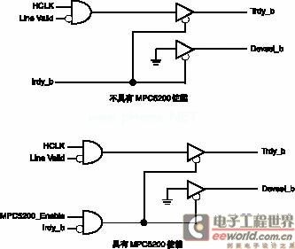
--- This example interface works only if no other real PCI target device is connected to the PCI interface. Otherwise, some supported types need to notify the interface logic to respond to upcoming PCI processing.
The 2:1 logic relationship of the -33MHz PCIclk and the 8.25MHz (or similar frequency) HCLK is shown in Figure 5.
â— In the 2:1 case, when HCLK is low, the sensor data is valid, and as the HCLK reappears as the next data shot, the next PCIclk edge will capture the data.
---PCI processing must be done before the LineValid judgment. PCI processing keeps waiting by Trdy_b when LineValid goes high. Since the 5200's enable signal requires rejection of several cycles, additional circuitry may be required at the end of the PCI process to shut down the circuit. In this process, people may require non-camera PCI processing (the interface logic must never respond).
â— Since HCLK is derived from the MPC5200 PWM, HCLK processing occurs after the PCIclk edge (PCIclk should arrive at the bus ahead of time depending on the design).
â— When HCLK falls, Trdy_b's judgment is delayed by one PCIclk.
â— When HCLK rises, Trdy_b also rises immediately.
• PCI data capture is created on the PCIclk edge, and then the PCIclk edge creates a rising HCLK as the pixels are increasing.
--- The BestComm task for controlling sensor data reading is very flexible and can be adjusted according to the size of the sensor. In this example based on a Freescale CMOS sensor, the resolution of the sensor is 640 x 480 pixels, 10 bits per pixel. After each line, the pulse stops and the BestComm task automatically begins reading the next line until the entire picture is completed. This method has a very high frame rate with an overhead of 15 clocks per line.
--- The overhead of transmitting 640 pixels of data is 640 clocks, plus the overhead of one line of 15 clocks, the total overhead of transmitting one line of pixels is 655 clocks. Each frame has 480 lines, and the required clock is 655 × 480 = 314400. If a 33MHz PCI clock is used, it takes 9.52ms to transmit each frame, that is, 105 frames per second. It can be seen from this that the frame rate depends on the resolution of the clock and sensor.
--- The length and number of pulses read for completing a complete picture are the parameters of BestComm, which can be adjusted for each type of sensor. The frame throughput achieved with the interface is much higher than the frame rate of the application. The limiting factor is the computational power required for the algorithm, which is closely related to the application.
Chip Display,Chips Display,Display Module,LCD Display Module,TFT Module
ESEN Optoelectronics Technology Co., Ltd, , https://www.esenoptoelectronics.com