Implementing AMP communication with Zynq SoC's on-chip memory
Last week we implemented the AMP (Asymmetric Multi-Process Processing) mode and implemented the system startup and operation on the ZynqSoC, and tried the most basic software applications on the ZynqSoC's two ARM Cortex-A9 MPCore processors. Now I want to explore how we can use ZynqSoC's OCM (on-chip memory space) to achieve communication between dual cores. In the previous 48 blogs of the MicroZed series, we have not seriously discussed OCM, but just passed by. Now we are going to use on-chip OCM, so we need to understand the on-chip OCM in depth. In fact, like other ZynqSoC on-chip resources, OCM is more powerful than its simple name.
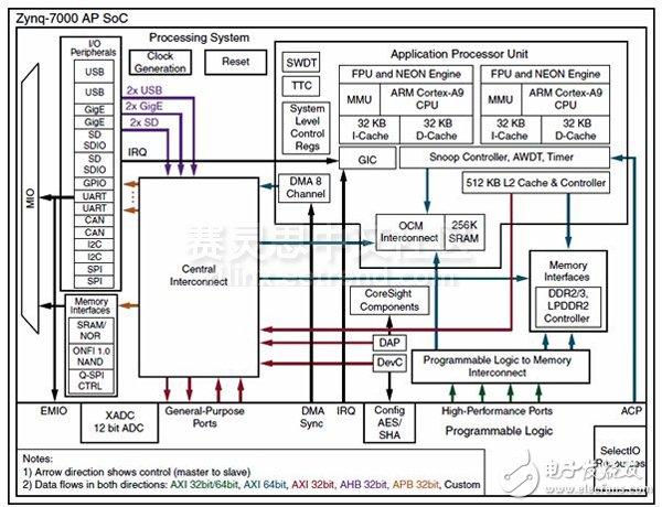
ZynqSoC has an on-chip 256K bytes of SRAM memory and has access to it in four sources. The following figure shows the structure of the Zynq PS (Processor System) section:
The following on-chip resources can access OCM:
1. OCM can be accessed by two ARM Cortex-A9 MPcore processors on the SCU (Listening Control Unit)
2. Access to OCM via the SXI (Listening Control Unit) PL (Programmable Logic) section using the AXI ACP interface
3. OCM can be accessed through the AXI High Performance interface through the PL part of the OCM interconnect structure.
4. Through the OCM interconnect structure, Central Interconnect can access OCM
So many different on-chip resources can access OCM, so it is very important to understand the OCM's operation and control methods before we use it.
Because the resources of such multiple multiplexing interfaces can access OCM, it is necessary to define the arbitration and priority mechanism of the access protocol. SCU read and write operations have the highest priority (read operations have higher priority than write operations). The read and write operations initiated by the OCM interconnect have the second highest priority. Note: You can override the priority of the SCU write operation and the priority of the OCM interconnect access by modifying the OCM control register to set the priority of the SCU write operation to a lower level.
The OCM can be organized into a 128-bit word storage space. The OCM storage space defined by the PS portion can be divided into four 64 kbyte storage locations at different locations. The initial configuration is to map the first three 64k bytes of memory blocks to the address space starting from the PS part. The last 64K bytes of memory blocks are mapped to the address space at the end of the PS part. You can view the address of the linked file in the figure below. The definition of space (the above picture shows the address space mapping of Core 0, the figure below shows the address space mapping of Core 1):
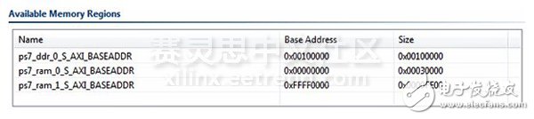
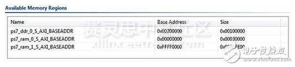
Note: ps7_ram_xxx and ps7_ram_1 are mapped to area 0 and area 1 of memory, not the address space of Core 0 and Core 1.
The address map of the OCM storage space is rewriteable, so it is completely contiguous and can be mapped to the end of the address space. You can use the system level control registers and the OCM configuration registers to configure the OCM memory address map space by setting the value of each bit of the appropriate RAM high.
OCM is a single-port storage space, but you can use ZynqSoC's DMA to access OCM's other switching resources to simulate a dual-port storage space. To implement this mechanism, the access must be 128-bit data alignment, regardless of the situation. This approach enables higher throughput because DMA can efficiently transfer large amounts of data.
If we apply OCM to a fairly demanding application, we can also add error protection mechanisms using the OCM parity control register. You can set the odd parity or parity check separately. Through this register, we can also configure how the ZynqSoC handles the parity error (by outputting the OCM shared interrupt 35 error or transmitting an AXI read, for example, when a read operation error is detected. Error (SLVERR) signal).

Optical Fibre Sensor,Optical Fiber Head,Optical Fiber Focusing Mirror,Optical Fibre Amplifier
Shenzhen ShenWu Sensor Co.Ltd. , https://www.szsuenw.com