Prediction of Loop Stability Technology Solution for UCC289X Active Clamp Forward Converter
1 Introduction
As power reliability assessments continue to evolve, the use of specific loop analysis instruments for loop stability testing is currently the only requirement. However, in the actual development process, engineers often spend too much time on loop stability function debugging. For example, when using an active clamp converter, we always run into loop stability problems because it is difficult to achieve a good balance between large signal load dynamics and small signal loop stability, especially This is especially true in peak current control mode. In terms of dynamic optimization of large signal loads, MOS voltage stress has a huge influence. In order to get better optimization, engineers usually spend a lot of time repeating debugging loop stability.
Since the small-signal model is not accurate, it is controversial whether this calculation method is suitable for actual measurement, but if an accurate small-signal model can be obtained, the problem can be solved.
The goal of this paper is to establish a computing platform to verify loop stability based on the improved CCM small-signal model of the active clamp forward converter used in the UCC289X application. Figure 1 shows an example of actual EVM verification. In addition, this article will provide you with a lot of comparison data. Finally, it has been proven that loop stability calculations are very useful for actual design and debugging during development when using UCC289X applications.
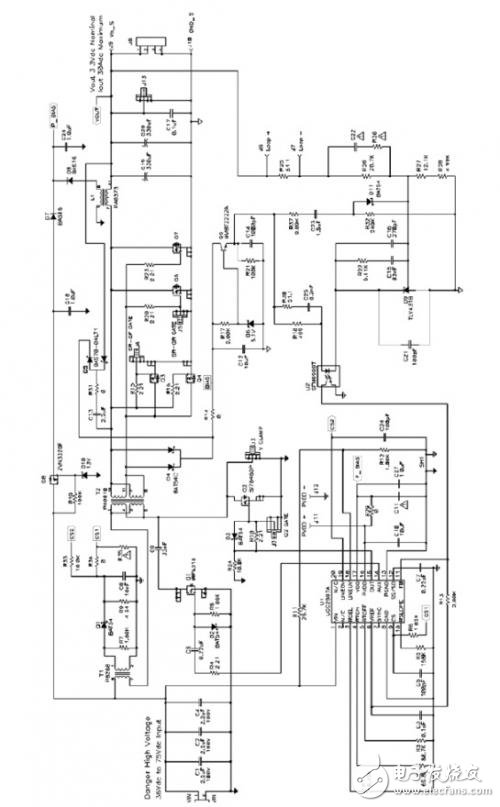
Figure 1 Schematic diagram based on EVM
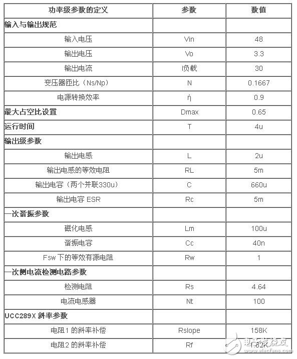
2, power level transfer function calculation
See the BOM of the schematic shown in Figure 1. The power stage parameters are listed in the table below.
Printed circuit boards which are used in medical industry.
The manufacturing method of the multi-layer board is generally performed by the inner layer pattern, and then formed into a single-sided or double-sided substrate by printing etching, and is incorporated into a specified layer, and then heated, pressed and bonded, as for the subsequent drilling. The hole is the same as the plated through hole method of the double panel.
The equipment and processes required for multi-layer boards are more complex and high-end. When designing the size of multi-layer boards, it is often necessary to consider more factors, especially the size of the equipment, whether it can allow such large size.
Medical Pcb,Medical Equipment Pcb,Medical Device Circuit Board ,Circuit Board For Medical Facility
Chuangying Electronics Co.,Ltd , https://www.cwpcb.com