Design of Wireless File Transmission System Based on nRF24L01 and FT245BM
The USB Universal Application Bus provides a high-speed, reliable transmission protocol for a large amount of data transmission between a USB device and a host. At present, U disk is widely used for file transfer between two computers, which is convenient and flexible to use, but it also has shortcomings. If some malicious viruses are hidden in the U disk, these viruses are likely to cause unnecessary loss to the user; in addition, when the amount of transmitted data is small, the repeated insertion and removal process will delay valuable time. Therefore, communication with a PC using a USB interface has its limitations. With the development of short-range wireless communication technology, more and more applications have been applied, such as instrumentation, computer telemetry and remote control systems, and home network systems. Both USB interface communication and wireless communication have their own advantages. If they are combined, they will have greater application prospects.
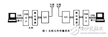
This article uses PIC16F877 single-chip microcomputer, USB chip FM245BM and wireless chip nR hole 4 function 1 to form a wireless file transmission system, making full use of the USB port data transmission function, the device is convenient to connect, and can carry out file bidirectional transmission.
1 main chip introduction1. Wireless transmission chip nRF24L01
24L01 is a single-chip RF transceiver chip, working in 2.4GHZ- 2.SGHz frequency band, working voltage is l.gV-3.6V, with up to 125 channels to choose from, the highest communication rate ZMb/, with automatic response and heavy Send function, its working parameters are all configured by chip status word. The microprocessor accesses the IDI via the SPI and writes the configuration status word to the IDI, which can be configured for transmit, receive, idle, and power-down modes. The chip has built-in frequency synthesizers, power amplifiers, crystal oscillators, modulators and other functional modules, and incorporates the enhanced ShockBurst technology. This technology is unique to IDI, which makes the two-way communication protocol simple.
1.2 USB chip FT245BM
The FT45BM chip is a second-generation USB chip introduced by FTDI. Its function is to realize the bidirectional transmission of data between the USB interface and the parallel 110 interface. It consists of a 3.3V regulator, USB transceiver, phase-locked loop, serial interface engine (SIE), nFO controller, USB protocol, nro receive buffer, transmit buffer, and 6MHZ oscillator, 8x clock Frequency multiplier and other components. On the one hand, when the external device has data to be transmitted to the host, the data is transmitted to the data buffer inside the USB chip through the 8-bit parallel 110 interface, and the På’«45BM converts the 8-bit parallel data into serial data, and the USB interface is used. The data is sent to the host; on the other hand, when the host has data to the external device, the serial data is first stored in the internal buffer of the USB chip through the USB interface, and the FT245BM converts the data into 8-bit parallel data, and then Data is passed to an external device via an 8-bit I/O interface.
2 system overall designThe core components used in this system are single-chip PIC 16F877, wireless chip nRF'24 function 1 and USB chip F1245BM. To transfer a file wirelessly from one computer to another, first convert the file to binary code (encoding), then wirelessly transmit it, then receive it wirelessly, and finally restore the binary to the original file (decoding). The encoding and decoding of the file is done by the computer VB program, and the hardware only performs the binary code transmission. Considering that the binary code is also relayed by the single-chip microcomputer, the USB chip FT245BM is connected between the single-chip microcomputer and the computer, and the wireless transmission is controlled by the single-chip microcomputer to the IDI. The overall block diagram of the system design is shown in Figure 1.
3.1 USB interface design
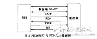
The control of the FT245BM by the single-chip microcomputer is completed by four read/write control signals of RXF#, RD#, TXE# and WR, as shown in Fig. 2. When RXF# is low, it means that the host has sent at least 1 byte of data to the receiving buffer of the USB. The MCU can read the data on D0-D7 to the MCU by simply setting the RD# signal from low to high. In the register. When TXE# is low, it means that the MCU can write 1 byte of data to the USB. Just turn the WR signal from high to low, and the data on D0 to D7 can be written into the USB transmission buffer. Note that when TXE# is high, the data cannot be written to USB. At this time, the data of the last write is being processed in the USB transmission buffer or the transmission buffer is full. Similarly, when RXF# is high, data cannot be read from the USB chip.
The circuit design can adopt bus power supply and self-power supply. The bus power supply mode means that the power of the På’«45BM device is supplied through the USB interface of the computer, and the current flows through the port into the PBA 45BM device. Self-powered mode means that the power of the R-port 45BM device is provided by itself and not by the host. If the bus power supply mode is adopted, a magnetic bead is used at the power supply end to reduce interference between the host and the device. At the same time, increasing the decoupling and bypass capacitors at the power supply terminal can improve the anti-interference of the circuit. If the circuit does not have an external EEPROM, the Rå’«45BM will use the default VID, PID, product descriptor and power descriptor.
3.2 wireless part design
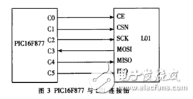
The connection diagram between the single chip and the work l is shown in Figure 3. CE, CSN, MOSI, MISO, SCK, and IRQ are control pins for L01. CE is the chip select terminal, CSN, MOSI, MISO, SCK are the SPI port of L()l, and PIC16877 and workl are communicated through SPI[2] port. SPI communication plays an important role in wireless transmission. For example, when the print 1 is to be configured, those configuration status words are written by the SPI port; when the data is to be sent, the address and the valid data are also written by the SPI port; when the IDI receives the data, The MCU also reads it through the SPI port, so the MCU must be connected to the Insulator 1 using SPI. The IRQ is the interrupt flag bit. The microcontroller can check the status of this bit to know if the transmission or reception is successful.
Cylinder Assembly,Cylinder Assembly Tubular,Cylinder Head Assembly,Clutch Master Cylinder Assembly
Chongqing LDJM Engine Parts Center , https://www.ckcummins.com