What is fpga? Fpga classic design and application: FPGA-based high-speed AD conversion system
As a programmable logic device, FPGA (Field Programmable Gate Array) is developed on the basis of logic devices such as PAL. It is relatively large in size and can replace hundreds of general-purpose IC chips. Its structure is mainly composed of three parts: a two-dimensional array of logic blocks, which constitutes the core of its logic; input/output blocks; and interconnection resources that connect logical blocks. With the continuous improvement of VLSI technology, the scale of FPGAs has become larger and larger, and its single-chip logic gates have reached millions of gates, and its functions have been continuously enhanced. Users can complete the design quickly and easily based on it. This design uses the chip EP2C35F672C6.
The use of FPGA to design digital system circuits has the following characteristics:
1) Design flexibility The FPGA is set up by the program stored in the on-chip RAM. Therefore, the on-chip RAM needs to be programmed during operation. Users can use different programming methods according to different configuration modes.
2) High integration level An FPGA can replace several, dozens or even hundreds of small and medium-sized digital integrated circuit chips.
3) Fast working speed The design idea of ​​FPGA is parallel design idea, not software idea of ​​sequential execution, which greatly improves the working speed of the system.
4) Reducing costs With the development of FPGA technology, FPGA has overcome its shortcomings of high price and has high cost performance.
In the radar design, the received signal is firstly subjected to analog-to-digital conversion. The conversion speed and accuracy directly determine the accuracy of the FFT and other operations, and ultimately affect the radar measurement accuracy. This paper introduces a kind of fast 14-bit serial AD conversion based on FPGA and uses chip ADS7890 to explain the software and hardware of the system. The hardware part is mainly the basic peripheral circuit of ADS7890 and the control connection of chip EP2C35F672C, and the software part is programmed by Quartus II 8.0.
Current real-time ranging technology includes ultrasonic ranging, laser ranging, and radar ranging. In principle, the above several ranging methods are similar, but the millimeter wave radar ranging overcomes some shortcomings in the application of several other detection methods. The millimeter wave radar has stable detection performance. Compared with optics, it is not susceptible to the shape and color of the object. Compared with ultrasonic and infrared rays, it is not affected by atmospheric turbulence and is affected by rain, fog and snow. The interference from sunlight, dust, etc. is small. The signal received by the radar is a frequency-modulated continuous wave signal. With the development of digitization, more and more analog signals need to be converted into digital signals for processing in the fields of detection and control. AD conversion is the process of outputting the input analog signal as a binary number. According to Shannon's theorem: If the highest frequency of the analog signal changes with time is ω, as long as the sampling frequency ωs ≥ 2ωmax is sampled, the sample taken out The series (f1*(t), f2*(t),...) is sufficient to represent (or restore) f(t). It mainly includes four processes of sampling, holding, quantifying and programming.
Corresponding to specific applications, AD conversion requirements are different. In high-frequency radar design, AD conversion requires higher conversion speed to achieve real-time ranging; and the accuracy of final radar ranging is directly related to the number of AD conversion and FFT bits. relationship. Some microcontrollers with AD not only have slow data processing speed, but also the AD digits are not up to standard. Therefore, this design uses FPGA-based platform to realize fast and high-precision analog-to-digital conversion using ADS78 90.
1 system hardware circuit
The main overall structure of the system is shown in Figure 1.
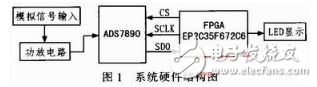
The system uses ALTERA's chip EP2C35F672C6 as the control core to control and convert the ADS7890 data processing. The radar rangefinder can be radar IVS-167, which is a K-band VCO radar transceiver with IVS (Innosent VCO stereo) series from Innosent. Due to the planar microstrip antenna structure and the combination of the transceiver antennas, the shape is very small, not only energy saving, but also easy to integrate into various circuits, and it is easy to construct module protection facilities in the installation environment.
In this design, the radar receiving signal is the analog signal input, the input signal reaches the AD conversion chip requirement through the power amplifier circuit, and then the FPGA is used to generate the timing control. The ADS7890 serially transmits the digital signal at the beginning and end, and processes the received data. After the result is displayed by led.
1.1 Chip ADS7890
The ADS7890 is a high-bit fast AD conversion chip that includes an analog 14-bit serial AD converter with an internal reference voltage of 2.5 V. The maximum sample rate is 1.25 MSPS with 48 pins for SPI or DSP interface. . The chip contains power-saving devices, and enters the power-saving mode when the conversion speed is low. The chip can be applied to photoelectric sensors, motor current/voltage sensors, medical testing instruments, high-speed data acquisition systems, and the like.
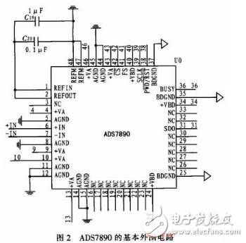
The basic peripheral circuit of the ADS7890 is shown in Figure 2. The analog ground is separated from the digital ground. ![]() The SDO 5 pins are connected to the control chip.
The SDO 5 pins are connected to the control chip.
2 system software design
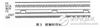
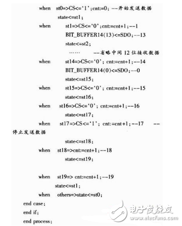
The basic control timing diagram of the FPGA is shown in Figure 3. The FS bit is the data frame format adjustment. When it is high, it is SPI mode. When it is low, it is DSP mode. This design is used for SPI and FS is set high. The falling edge of CS triggers the ADS7890 to transmit data, and sends one bit of data on the rising edge of SCLK. The 14 pulses correspond to the 14-bit result of AD conversion, and then use 1 and 2 SCLK cycles as the delay to ensure the correctness of the AD result. Set a BUSY as a busy flag and do not accept data after setting it high. Set a reset bit RESRT. SDO is the data transmission bit.
The programming design uses the VHDL language. VHDL is primarily used to describe the structure, behavior, functions, and interfaces of digital systems. In addition to statements that contain many hardware features, VHDL's linguistic form and descriptive style and syntax are very similar to general computer high-level languages. A complete VHDL language program usually contains five parts: EnTIty, ArcbAtecture, ConfiguraTIon, Package, and Library.
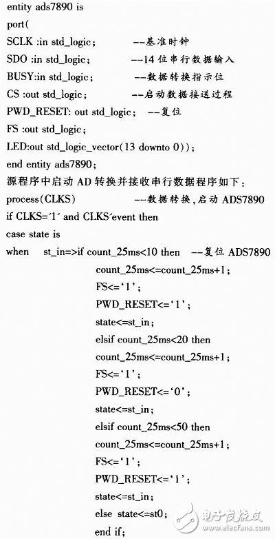
The structure in the source program is defined as follows. Note that the input to the ADS7890 corresponds to the output of the EP2C35F672C6.
3 Conclusion
With the development of digitalization, AD conversion has been fully applied in various fields, and its requirements are getting higher and higher. This design uses a highly integrated FPGA as the hardware platform to realize the control application of the high resolution analog-to-digital conversion chip ADS7890. It has high conversion accuracy through actual test, and is sensitive to fast-changing input signals. The system test is accurate and stable. reliable.
UV Screen Protector,UV Curing Machine,UV Curing Screen Protector
Shenzhen Jianjiantong Technology Co., Ltd. , https://www.jjthydrogelprotector.com