FPGA internal module working principle VGA and XGA timing introduction in VESA standard
ARM is currently the world's largest IP provider of embedded chip technology, and its IP has become a technology standard and development platform adopted by many chip design companies. Therefore ARM core-based SoC development has become the focus of embedded processors, may be implemented to complete the LCD controller controls the LCD panel through the embedded ARM. If the TFT screen is used to support display, its image resolution has limitations. Therefore, by setting up an FPGA platform, the image scaler function is externally connected to the LCD display to complete the extended display of the ARM signal. At the same time, the FPGA can also verify and simulate the image signal generated by the ARM platform to test the correctness of its function and timing. XGA display has become a common output device in most designs due to its large display volume and various output forms. Therefore, the VGA signal generated by ARM is extended to XGA standard signal by interpolation algorithm.
1 VGA and XGA timing in the VESA standardThe Video Electronics Standards Association (VESA) is a non-profit international organization that develops video interface standards for personal computers, workstations, and consumer electronics. Therefore, the VGA and XGA timings designed in this paper are designed in accordance with VESA standards.
The display usually adopts a progressive scan mode, and each frame image is continuously scanned one by one and one row in sequence, and the scanning is controlled by the horizontal synchronization signal HSYNC and the vertical synchronization signal VSYNC during scanning. The timing chart of line scan and field scan is shown in Figure 1. The timing requirements of line scan and field scan are shown in Table 1 and Table 2.
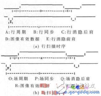
Figure 1 Line scan timing and field scan timing
2.1 system block diagram
The data source for the system design is the video signal from the ARM9 system board. The format is VESA standard VGA signal. After the data source enters the FPGA, image scaling is performed first, and the input effective pixel data is processed by an algorithm. The processed data is buffered by FIFO and DDR2, and then the processed image data is sent to the video encoding according to the XGA timing. The chip is finally sent to the display. The FPGA internal design is divided into timing control module, timing generation module, FIFO module, image scaler module and DDR2 SDRAM controller module, as shown in Figure 2.
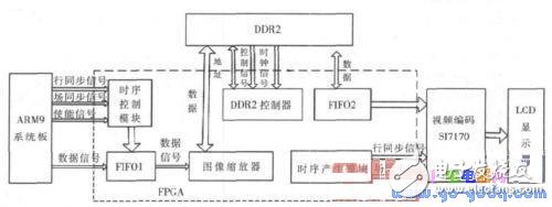
Figure 2 System block diagram
2.2 Hardware implementation
The FPGA uses ALTEra's EP3C16F484C6 chip, which has 15 408 logic cells, 504 KB of memory, 56 multipliers and 4 PLL phase-locked loop cores. It supports up to 346 I/O ports with a system clock of up to 250 MHz. The FPGA development board uses a dedicated video decoding encoding chip. SILICon Image's video encoding chip SI7170 ​​supports VGA to UVGA format standards, and also supports HDTV format encoding. DDR2 SDRAM uses Samsung's K4T51163QC chip, and its frequency supports 267 MHz. This article chooses 200 MHz. The chip capacity is 32 MB & TImes; 16, in fact, as long as the SDRAM satisfies the capacity of storing 2 frames of images, it can meet the design requirements of this paper [1]. The output clock required to complete the converted XGA signal is 65 MHz and can be generated by the FPGA's internal phase-locked loop.
3 FPGA internal module works3.1 input timing control module and output timing control module
The input timing control module ensures that valid image data can be successfully written to the FIFO for buffering based on the synchronization signal and timing requirements of the input video signal. For example, when the module receives the field sync signal, the FIFO enters the state to be written. When the module receives the enable signal, the FIFO starts writing data, which ensures that the data written to the FIFO starts from the beginning of the complete 1-frame image. Write.
The function of the output timing control module is to generate the synchronization signal, the field synchronization signal and the line synchronization signal necessary for outputting the image to ensure that the data of the output image is consistent with the timing, so that the image can be correctly displayed on the display.
The input and output timing control module is designed according to the counter method [2]. For example, the total pixel requirement of a 1-frame image of a VGA signal is 800 & TImes; 525, where the effective pixels are 640 & TImes; 480. For line scanning, 1~96 pixel clock count can be set as line sync signal, 97~144 pixel clock count is line blanking back shoulder, 145~784 pixel clock count is image effective pixel display, 685~800 pixel clock count is Line blanking the front shoulder. After completing one line, the counter is set to 0, waiting for the new line sync signal to arrive and recount. In the image effective pixel clock, the write FIFO enable signal is in an active state, and the remaining time enable signal is in an inactive state, thus ensuring that valid image data can be accurately written into the FIFO for buffering, and waiting for the next processing.
3.2 Image Scaler Module
As shown in FIG. 3, the image scaler module mainly performs scaling of the resolution of the input image data source. According to the design, the input image data is VGA 640&TImes; 480 format, and the output image data is XGA 1024×768 format. Since the ratio of the input image data to the output image data in each row of pixels and the number of columns in the complete 1 frame is 5:8, a 5:8 amplification of the input VGA signal can be considered. First, the data is interpolated and enlarged in the horizontal direction, and then amplified in the vertical direction. The interpolation and amplification in the horizontal direction and the vertical direction in the design all use the hierarchical bilinear interpolation algorithm.
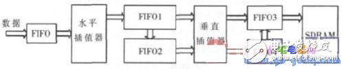
Figure 3 image scaler module block diagram
3.2.1 Hierarchical bilinear interpolation [3]
In the bilinear interpolation algorithm, the value of the interpolation point is calculated according to its four adjacent known points, as shown in FIG.
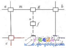
Figure 4 Schematic diagram of bilinear interpolation algorithm
It is known that a, b, c, and d are adjacent four points in the input image, and the gradation value thereof is represented as f(x). The fractional part of the coordinate value after the pixel f to be inserted is mapped to the original image is [m, n]. The process of calculating the gray value of the f-point is as shown in equations (1) to (3):
f[g]=f[a]+m(f(b)-f(a)) (1)
f[h]=f[c]+m(f(d)-f(c)) (2)
f[f]=f[g]+m(f(h)-f(g))
=(1-m)(1-n)f(a)+m(1-n)f(b)+(1-m)nf(c)+mnf(d) (3)
The four source image pixels used for hierarchical bilinear interpolation are the immediate neighbors of the points to be interpolated. The calculation process of interpolation is as follows:
g(x)=(f(a)(m×N)+f(b)×(1-m)N)/N
Where m and 1-m are the weights of points a and b, respectively. Because it is a 5:8 conversion, here C = N = 8, the length interval of the original 5 pixels is divided into 8 intervals, each of which has m × N and (1-m) N An integer pair of weights. The points to be interpolated inside each interval take the same value as the left boundary of the interval. The weights of the eight intervals correspond to (8,0), (7,1), (6,2), (5,3) (4,4), (3,5), (2,6) and 1,7). After determining the position of the point, the relationship between the weight and the position is written in the manner of a lookup table. Finally, the corresponding coefficient can be found according to the relative position of the interpolation point and the adjacent point, and the gray of each pixel point is calculated by calculation. Order value.
3.2.2 Specific interpolation process
3.2.2.1 Horizontal interpolation
The bilinear interpolation is decomposed into horizontal and vertical directions. Since the original image is amplified by 5:8, according to the hierarchical bilinear interpolation, the 5 pixels in the original horizontal direction are divided into 8 levels of bilinear interpolation. Feed in the horizontal interpolator. The horizontal interpolator is controlled by the counter and the enable signal at the same time. Each interval is 5 clocks, the horizontal interpolator enable is placed in the calculation interpolation state, and the entered 5 values ​​are interpolated into a new 8 pixel points, and then After 5 clocks, the new value is entered into the interpolator for interpolation until 1 line of 640 pixels is interpolated into 1 line and 1 024 pixels.
3.2.2.2 Vertical interpolation
The vertical interpolator completes the 5:8 conversion in the vertical direction, that is, the conversion of 5 lines of data into 8 lines of data. The interpolation process uses 8 levels of bilinear interpolation for the original 5 lines of data in the vertical direction, and transforms into a new 8 Row data.
The data pipeline type that completes the horizontal interpolation passes through the FIFO1 and FIFO2 modules. During the period, the values ​​of FIFO1 and FIFO2 are sent to the vertical interpolator for interpolation, and the data after the vertical interpolation is sent to the FIFO3 and FIFO4 modules, and the output is sequentially arranged in the FIFO3. And another row of data enters FIFO4. The data between FIFO3 and FIFO4 is also pipelined into the DDR2 SDRAM module. The whole process controls the vertical interpolation by using the state machine, so that the vertically interpolated data can be interpolated in the correct order and sent to the DDR2 SDRAM module. . The time when the original 5 lines of data are horizontally and vertically interpolated into 8 lines of data is taken as one cycle until the enlargement of the entire frame of the VGA format image to the 1 frame XGA image is completed.
3.3 DDR2 SDRAM Controller Module
The specific function of the controller module is: when SCALER completes the image data processing, the image data is sent to the DDR2 for storage. When it is ensured that 2 frames of the complete image are stored in the DDR2, the read end of the DDR2 starts to read, from the first The frame image address reads the image data and then outputs it from DDR2 according to the timing control. After reading the first frame, continue to read the second frame, at which time the third frame continues to write the original first frame address, and subsequent read writes are performed according to this process.
Since DDR2 SDRAM cannot be written and read at the same time, it needs to be controlled by a DDR2 SDRAM controller. The read and write control can be performed according to the amount of data stored in the FIFO connected to the write end and the read end of the DDR2 SDRAM module. The FIFO before the write end is the FIFO3 of Figure 3. The FIFO connected to the DDR2 readout is FIFO2 of Figure 3, which together with the output timing control module completes the output of the final desired XGA image. Each time the DDR2 SDRAM operates an instruction, it takes one line of data, that is, accepts one read command, and reads one line of data. Similarly, when one write command is accepted, one line of data is written, and the one line of data is simultaneously 1 line for the XGA format (1 024 pixels of data).
4 simulation and function realizationIn the design, the Verilog language is used to design and design each logic module. In the development environment QUARTus II 9.1 and Modelsim-aLTEra 6.5b, the simulation and function design and verification of the timing of each module are completed, as shown in Figure 5. After entering the horizontal interpolator simulation results, the horizontal interpolation inserts the original 5 pixels into a new 8-pixel simulation, where pix is ​​the 5 pixels to be interpolated, and data is the 8 new pixels after interpolation.
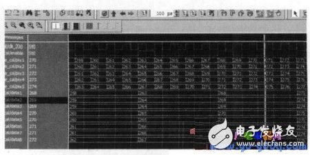
Figure 5 Horizontal interpolation of 5 pixels into 8 pixel Modelsim simulation
After the simulation of each module design, and the function verification of each module is correct, the whole system is simulated and verified, and finally the processed image data is sent to the LCD for display. The enlarged example is shown in Fig. 6. The simulation verification shows that the obtained image timing and data are consistent with the required timing. For the image data, although the bilinearity will have high-frequency component loss on the edge of the screen [4], the outline is slightly blurred, but from the image The impact of human viewing is small.

Figure 6 Display of the amplified ARM image signal on the LCD (XGA format)
The VGA and XGA timings in the VESA standard are introduced. The image scaler is designed through the FPGA platform to complete the simultaneous input and control of control signals, timing signals and data signals. At the same time, the interpolation algorithm is used to amplify the resolution to achieve the ARM image signal. The extension is displayed. To achieve more conversion between formats, you can write algorithms between various image format scaling, such as VGA, XGA, SVGA and other formats. In the program, the state machine is used to realize the conversion and timing control between different formats, and the scope of the zoom is enhanced to expand its application.
Heart Rate Smart Watches
Heart Rate Smart Watches,Smart Watch Heart Rate Monitor,Smart Heart Rate Wristband,Smartwatch Heart Rate
everyone enjoys luck , https://www.eeluck.com