Design and implementation of intelligent power supply in vehicle unit
The research field of Intelligent Transportation System (ITS) is the development direction of the future transportation system. It is the effective integration of advanced information technology, data communication transmission technology, electronic sensing technology, control technology and computer technology. The ground transportation management system establishes a comprehensive, real-time, accurate and efficient integrated transportation management system that functions in a wide range and in all directions.
This article refers to the address: http://
1 Introduction to ETC System
Electronic Toll Collection (ETC) is designed as a Road Side Unit (RSU), OnBoard Unit (OBU), IC card, computer security control technology, network and accounting. Most of the composition.
Its composition is shown in Figure 1.1:
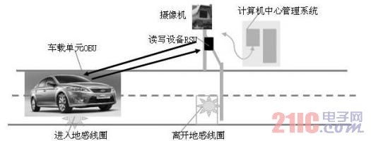
Figure 1. 1 ETC system composition diagram
The OBU contains the identification information of the vehicle, such as the license plate number and the car ID number, which are usually installed on the windshield in front of the vehicle. The RSU is installed next to the toll booth, and the loop sensor is installed under the driveway floor. The central management system has a large database that stores information on a large number of registered vehicles and users. When the vehicle passes through the toll gate, the loop sensor senses the vehicle, the roadside unit sends an inquiry signal, and the onboard unit responds. The two-way communication and data exchange are carried out, and the central management system obtains information such as vehicle identification and vehicle type and compares and judges corresponding information in the database, and controls the management system to generate different actions according to different situations. The roadside unit communicates with the onboard unit to exchange information and exchange information to achieve automatic identification of the vehicle, and automatically deducts the toll from the user's dedicated account, thereby realizing automatic charging.
Because the OBU plays a very important role in the entire ETC system, the performance of the power module is directly related to whether the OBU can work normally. There are two types of existing OBU power supply methods, but each has its own shortcomings. Accordingly, new low-power power supply design methods should be produced.
2 Low-power intelligent power supply application design scheme in electronic non-stop charging system
For example, an embedded processor-centric system such as OBU is mainly composed of processor power consumption and peripheral circuit power consumption. Considering the actual operation, the time of passing through the toll booth is very short during the whole process of driving on the road. The OBU only needs to work when the car passes through the toll booth, and the working time is less than one second. Time does not need to work. OBU intelligent power management uses a battery-powered method to control the OBU to operate in two modes, sleep mode and active mode; when the car enters the toll booth, the OBU is activated, starts working, is in active mode; when the transaction is completed, the car leaves the toll booth After that, the OBU immediately stops working and enters sleep mode. According to this feature, the strategy of hierarchical management of the power supply is divided into standby power supply and working power supply, as shown in Figure 2.1.
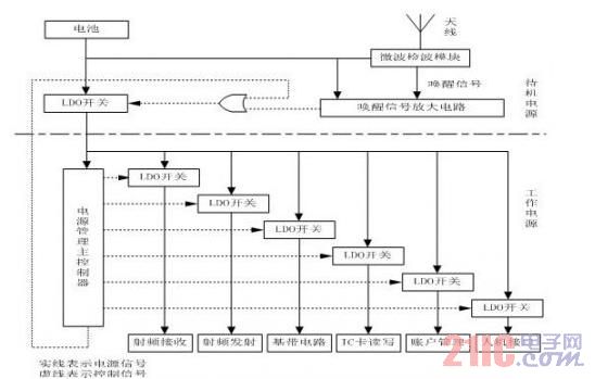
Figure 2. 1 OBU power management classification module structure
At the same time, in order to realize further time-sharing power supply control, the working power module divides the independent power supply loop according to the functional modules, and the power of each module is independently controllable, and is coordinated by the main controller.
The activated MCU uses interrupt writing mode to judge each I/O and time-sharing control, and outputs DC/DC enable high-level signals of each power consumption module. Time-sharing is RF receiving, RF transmission, baseband circuit, and IC. Card reading and writing, account management and human-machine interface power supply; at any time, the system only supplies power to at most 2 modules except the main controller, which greatly reduces the power consumption of the system.
3 intelligent power circuit design and device selection
3.1 Amplifier circuit design
The signal detected from the detector is very weak, it may be a few milliamperes or even a microampere level. Such a small signal generally cannot meet the signal amplitude requirements of various circuits in the latter stage, so it must be amplified. The quiescent current of the op amp is proportional to the bandwidth. The larger the bandwidth, the larger the quiescent current. This can be clearly seen in the selection tables of major semiconductor manufacturers. By comparison, in order to design a large gain. The amplifier with small noise and a certain bandwidth, this design selects TLV2382 as the most wake-up signal amplifier.
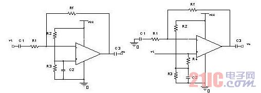
Figure 3. 1 Operational amplifier single-supply circuit
3.2 Low Power MCU Software and Hardware Design
In order to achieve low power consumption, MCU should choose its own low power consumption model, an ultra-low power MCU, which is mainly considered from the following aspects: system average current, clock system, interrupt, on-chip peripheral, BOR protection, pin Leakage current, processing efficiency. Based on this feature, the design selected a 16-bit ultra-low-powered Mixed Signal Processor MSP430 series of microcontrollers that Texas Instruments (TI) introduced to the market in 1996.
3.3 System clock design
For a system with low voltage sleep wakeup, the choice of crystal is very important. This is because the low supply voltage reduces the excitation power supplied to the crystal, especially when the sleep wakes up, causing the crystal oscillator to start slowly or not start at all, and the long startup time will significantly increase the power consumption of the system. The system designed by MSP430F2001 can solve this problem well.
The low-speed clock uses 12kHz VLOCLK, and the high frequency is generated by the internal integrated DCO oscillator. The appropriate output frequency can be selected by adjusting the control parameters.
3.4 Power supply design
The system uses 2 dry cells as the test power supply, and generates +3.3V voltage through the power chip. Since the input voltage range of the TPS79633 is 2.7~5.5V, the enable signal is high level and low level, so the I/O pin of the microcontroller can be directly used as the enable signal.
The operation of the MCU is completely determined by the output POW of the main switch, and the MCU only switches between working and power-off. Other I/O interfaces are used to control the output of the remaining modules for time-sharing control.
3.5 Software Design
In terms of reducing power consumption, it is necessary to combine hardware and software to achieve the desired effect. The software design mainly pays attention to the following aspects:
The system uses interrupt writing mode to judge each I/O, time-sharing control, and time-sharing power supply for each module to reduce power consumption. Secondly, a feedback signal is output to control the main switch to achieve the function of power off.
The power consumption of the system increases as the frequency of the system increases. Using the 12 kHz master clock after the system starts operating can reduce the power consumption during operation.
4 Conclusion
The low-power design of embedded systems is a design principle that must be considered in embedded system design. A successful low-power design should be a combination of hardware design and software design. From the hardware design, you should be fully aware of a low-power The characteristics of the application, choose a suitable MCU, through the understanding of its characteristics, design the system solution; in the software design, we must consider the special nature of low-power programming, and try to use the low-power mode of the microcontroller.
Feyvan Electronics designs and manufactures NTC temperature sensors, probes, and cable assemblies with excellent long-term stability, high accuracy and short response time in high-temperature sensing applications such as automotive, home appliance and industrial use from -40℃ to +250℃.
With more than 15 years of NTC thermistors and sensor probes production experiences, Feyvan electronics provide various choices for a wide range of applications and are available in custom engineered probe package configurations for a variety of mounting and connectivity options with low costs.
Medical Equipment Sensor
Medical Equipment Sensor,Medical Sensor,Sensors Used In Healthcare,Medical Equipment Temperature Sensor
Feyvan Electronics Technology Co., Ltd. , http://www.fv-cable-assembly.com