Explain the design skills of high-power LED lighting
The general LED lighting lamp has a current limiting resistor in the driving circuit, and the power consumed by the resistor has nothing to do with the LED lighting. In order to improve efficiency, it is necessary to use a constant current output switching power supply, and the use of power MOSFETs in the output stage.
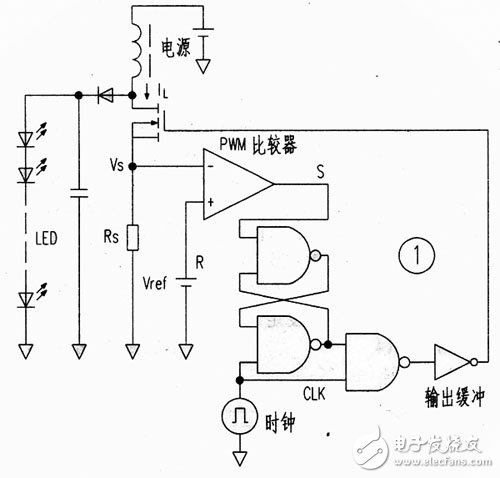
Figure 1 is a block diagram of such a driving circuit, which omits the triangular wave generator and error amplifier of the conventional circuit, and uses a CMOS logic IC and a PWM modulator. When the clock CLK signal is low, the RS flip-flop is in a reset state, and the output FET is turned off. When the CLK signal is high, the output FET turns on. Its current is converted into a voltage by the resistor Rs. When this voltage is higher than the reference voltage Vref, the comparator output changes from high to low, the RS flip-flop is reset, and the output FET is turned off again. As a result, even if the power supply voltage changes, the energy stored in the inductor is constant. Constant power output is achieved. Here, the voltage drop on Rs is used as the triangle wave voltage, and the PWM comparator directly compares this voltage with the reference voltage and functions as an error amplifier.
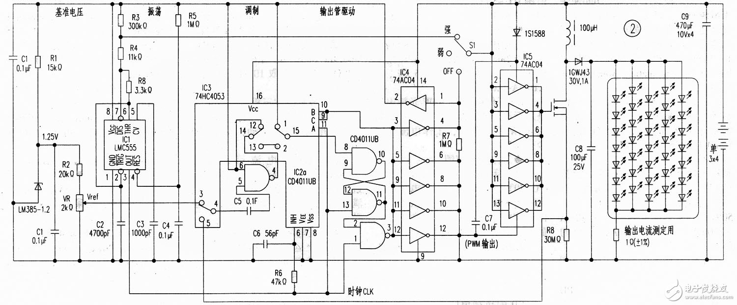
The actual circuit is shown in Figure 2, which uses discrete components, with a focus on the PWM comparator and voltage-doubled pulse output circuit.
The PWM comparator consists of a NAND gate IC2a ​​and an analog switch IC3, a so-called chopper comparator, and sets an input terminal of the NAND u7yh to a high level to become an inverter. The inverter repeatedly works in two states of "precharge" and "comparison".
Precharge state
In the pre-charge state, the capacitor C5 is charged by the reference voltage Vref provided by IC6 (LM385), and the output is neither high nor low; instead, it remains in the output state when the comparator is about to flip and triggers with ItS The device is combined into a PWM circuit.
Comparison status
The input voltage shifts the voltage level charged on C5, and is input to the inverter, compared with the threshold voltage of the inverter, and outputs a high level or a low level.
Voltage double pulse output circuit
As the name implies, this is to generate a pulse that is twice the power supply voltage. First of all, when inputting low level, the capacitor C7 is charged and the output is 0V; when inputting high level, voc and the voltage on the capacitor are connected in series, and the voltage at the YlX terminal of the inverter IC5 is 2Vcc; voc voltage, so output 2Vcc.
In Figure 2, the 555 (IC1) time-base circuit generates a clock pulse, and changes the charging voltage of C2 through the brightness adjustment switch 51 to select the 11.2kHz and 965Hz two-block frequency to change the clock frequency to achieve the purpose of changing brightness.
The output circuit and PWM comparator are directly connected to the power supply, but the power consumption is only 10uA per day without lights.
The output is connected with 35 white light diodes, divided into five groups in series and parallel.
Electronic Cigarettes,Electronic Cigarettes Starter Kit,E Cig Electronic Cigarette,V2 Electronic Cigarettes
Dongguan Fangbei Electronic Co.,Ltd , https://www.connectorfb.com