The principle of the board - it is so capricious
Guide: You may be familiar with the circuit board, but do you know how it actually works? If not, take a moment to read through this article and expand your technical knowledge!
1. Circuit Board Principles – Introduction
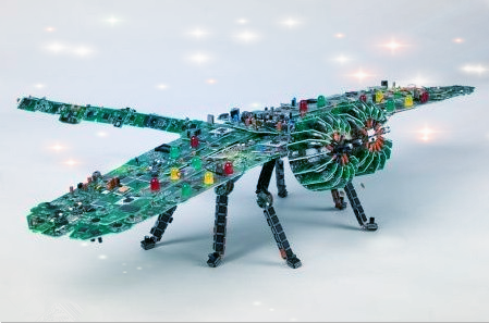
A printed circuit board, commonly known as PCB, is a critical component in modern electronics. It serves as a base for mounting and connecting electronic components. PCBs are made using copper etching technology, where conductive paths are created on an insulating substrate. With the miniaturization of electronic devices, many boards now use advanced techniques like film-based etch resists and photo-exposure processes to create precise circuit patterns.
2. Circuit Board Principles – Structure
A typical PCB consists of several key elements such as pads, vias, mounting holes, traces, components, connectors, and more. Common types include single-layer, double-layer, and multi-layer PCBs. Here’s a breakdown of their functions:
- Pad: A metal area used for soldering component leads.
- Via: A conductive hole that connects different layers of the board.
- Mounting Hole: Used to secure the board in place.
- Trace: A copper line that connects component leads and forms the electrical path.
- Connector: Allows connections between different boards or modules.
- Fill: Helps reduce impedance by providing a ground plane.
- Electrical Boundary: Defines the physical limits of the board, ensuring all components stay within this area.
3. How a Circuit Board Works
The core principle of a circuit board is to isolate the conductive copper layer from the insulating material. This allows current to flow along pre-designed paths, enabling functions like signal amplification, filtering, modulation, and more. On a basic PCB, components are usually placed on one side, while the wiring is on the other. These are called single-layer boards. For more complex designs, multi-layer boards use vias to connect different layers electrically.
The process of designing a PCB typically involves four main steps:
- Circuit Schematic Design: Create a schematic diagram using software like Protel DXP.
- Generate Network Report: This report shows the relationships between components and is essential for PCB layout.
- PCB Layout Design: Convert the schematic into a physical layout, which is more complex than the schematic design.
- Generate Reports: After the design is complete, generate various reports and print the final PCB layout.

Understanding the principles of circuit boards is essential for anyone interested in electronics. Here are some related articles you might find interesting:
- 1. PCB Design Tips: Learn how to quickly create a board
- 2. Secrets of a Circuit Board Enthusiast
- 3. How to Make Your Own Circuit Board at Home
Battery For Pesticide Spraying Drone
Battery For Pesticide Spraying Drone,Drone Batteries For Agriculture,Battery Of The Spraying Drone,Battery Type Of Drones
Shenzhen Jentc Technology Co., LTD , https://www.phenyee.com