Set the common-mode input voltage range of the high-speed ADC (Chinese)
Set the common-mode input voltage range of the high-speed ADC (Chinese)
For communication receivers that include baseband sampling and high-speed ADCs, the input common-mode voltage range (VCM) is very important. This problem is especially critical for single-supply, DC-coupled low-voltage systems.
For a single-supply power supply circuit, the input signal to the drive amplifier and ADC should be biased in the VCM range, thereby eliminating the performance barriers of the amplifier and ADC, because the amplifier and ADC do not need to maintain low distortion and high linearity at 0V.
In a typical direct conversion radio frequency receiver, a high-speed ADC usually uses a differential, DC coupled input. The design uses a zero-IF (ZIF) architecture with an RF quadrature demodulator and two baseband ADCs. The ZIF circuit is widely used by designers because it eliminates multiple IF down-conversion and SAW filters. Most ZIF architectures use DC coupling because the bandwidth of the in-phase (I) and quadrature (Q) signals they receive is close to DC. In addition, DC coupling can also eliminate the large-scale coupling capacitor between the RF downconverter and the high-speed ADC. It also eliminates the power-up delay caused by the discharge of the coupling capacitor.
The importance of VCM for ADC can be further understood from the following factors:
When the power supply voltage (VDD) changes, the output range of the RF quadrature demodulator varies greatly, which directly affects the common-mode input voltage of the ADC.
Common-mode input voltages that exceed the ADC VCM range produce harmonic distortion, which reduces the dynamic range. Correct VCM DC bias helps optimize the linearity of the amplifier and ADC, reduce distortion, and improve the bit error rate (BER).
In Figure 1, the UI can simplify the DC coupling, differential analog interface between the RF front-end and the drive amplifier, ADC. The circuit includes: two 8-bit, 40Msps ADC (U1) and two four-channel, single-supply broadband amplifiers (U2-U3), which can adapt to RF quadrature demodulator (differential, DC coupled signal source) and high-speed ADC Wider common-mode voltage range between requirements. The ADC provides sufficient signal / noise + distortion ratio (SINAD) and spurious-free dynamic range (SFDR) for demodulating a 3.84MHz broadband QPSK communication link. U2 and U3 should meet the requirements of SFDR and input common-mode voltage range. When a single 3V power supply is used, U1 consumes 90mW of power. 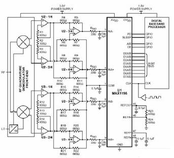
Figure 1. High-speed ADC (U1) uses its COM output to accurately set the common-mode voltage
The simplified VCM conversion circuit is the DC common mode output of U1 (COM, pin 1), REFIN (pin 46), and REFOUT (pin 45). COM provides a DC output (VDD / 2) consistent with the common-mode voltage range of the U1 input, and is independent of changes in VDD. REFIN and REFOUT set the full-scale range of the ADC through the resistor divider R23-R24, thereby optimizing the SFDR of the input amplifier and the dynamic range of the ADC.
U2 and U3 are configured as DC-coupled differential inputs and outputs, with a gain of 15dB, which provides the ADC with a full-scale (FS) input of 1VP-P. In order to maintain the dynamic range of the receiver, when selecting U2 / U3 amplifiers, their SFDR is required to be 10dB better than the ADC's 48.7dB SINAD. The FS voltage of U1 is set by R23 and R24:
FS = R24 / (R23 + R24) x REFOUT. (REFOUT = 2.048V)
The COM voltage (pin 1 of U1) is equal to VDD / 2 or 1.5V (when VDD = 3V). This voltage is also equal to the input VCM range of U1. In this way, when VDD changes with temperature and power supply voltage, COM and VCM track each other to ensure that the correct DC voltage is obtained. The COM pin can source 5 mA of current, and other DC voltages of the system can be set if necessary. Because the internal buffer of the COM is turned off when the ADC is turned off, using this level setting can save more power, which is better than the continuous power supply scheme provided by the dual resistance voltage divider.
The typical application circuit shown in Figure 1 is a WCDMA receiver, and the input signal rate of each ADC is half of 3.84 Mcps. When the signal is oversampled by U1 at a quadruple rate (Fclk = 15.36MHz), it has two advantages: First, oversampling places the mirror frequency between 13.44MHz and 17.28MHz (FI = Fs ± Fa), simplifying The design of the aliasing filter; secondly, oversampling provides a processing gain of 6dB: SNR = 10log (Fs / 2BW).
The digital output circuit of U1 is powered by OVDD = + 1.8V, which helps to save power. The + 1.8V bus reduces the digital signal swing. According to the relationship: P = CV2F (for each 8-bit bus), it can be seen that the power loss can be greatly reduced. The digital output of U1 is multiplexed, allowing a single 8-bit bus to interface with a dual-channel 8-bit ADC. The multiplexer helps reduce the number of digital I / O pins, saves board space, reduces ASIC costs, and improves system reliability.
Other options: MAX1185 is a dual-channel 10-bit ADC, and the pins are compatible with MAX1196. Both chips are available in 7mm x 7mm, 48-pin TQFP packages with exposed pads. The MAX1192 is an ultra-low-power, small-size, dual-channel 8-bit ADC that consumes less than 25mW at 3V. It is packaged in a 5mm x 5mm, 28-pin QFN.
Kitchen Hob,Gas Hobs,Gas Cooker Hob,Four Burner Gas Stove
xunda science&technology group co.ltd , https://www.gasstove.be