TDA7440D sound processing circuit
The TDA7440D is a dual-channel audio signal processing IC with I²C bus control capabilities. It's widely used in audio systems for advanced signal handling and tuning. The application circuit is illustrated in Figure 1-3, and the pin functions are as follows:
Pin 1 (RIN3) – This is the third input for the right channel audio signal, but it is not used in this particular design.
Pin 2 (RIN2) – This serves as the second input for the right channel audio signal, typically used to receive external AV signals. An external capacitor C2513 (470nF) is connected for coupling purposes.
Pin 3 (RIN1) – This is the first input for the right channel audio signal, used to receive TV audio from the CN8206 pin. A 470nF coupling capacitor, C2510, is connected externally.
Pin 4 (L_IN1) – This is the first input for the left channel audio signal, also receiving TV audio from the CN8206 pin. An external 470nF capacitor, C2511, is used for coupling.
Pin 5 (LIN2) – This is the second input for the left channel audio signal, used to receive external AV signals. An external 470nF coupling capacitor, C2512, is connected.
Pin 6 (L_IN3) – This is the third input for the left channel audio signal, but it is not used in this configuration.
Pin 7 (LIN4) – This is the fourth input for the left channel audio signal, but it is also unused in the system.
Pin 8 (MUXOUT/L) – This is the left channel output of the MUX block. It is connected via a 22μF capacitor to Pin 9.
Pin 9 (IN/L) – This is the left channel audio input, which is derived from Pin 8.
Pin 10 (MUXOUT/R) – This is the right channel output of the MUX block, connected through a 22μF capacitor to Pin 11.
Pin 11 (IN/R) – This is the right channel audio input, sourced from Pin 10.
Pin 12 (BIN/R) – This is the B signal input for the right channel, with an external 100nF coupling capacitor, C2664.
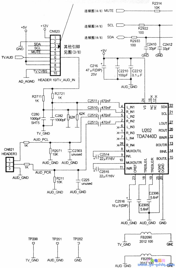
TDA7440D Audio Processing Circuit and TDA7268 Dual Audio Power Amplifier Output Circuit (a)
Pin 13 (BOUT/R) – This is the B signal output for the right channel, with an external 100nF coupling capacitor, C2662. Pin 14 (BIN/L) – This is the B signal input for the left channel, connected with a 100nF coupling capacitor, C2660.
Pin 15 (BOUT/L) – This is the B signal output for the left channel, with an external 100nF capacitor, C262.
Pin 16 & 17 (NC) – These pins are not used in the current design.
Pin 18 (TREBLE/L) – This is the high-frequency filter for the left channel, with an external 5.6nF capacitor, C2305.
Pin 19 (TREBLE/R) – This is the high-frequency filter for the right channel, using an external 5.6nF capacitor, C2306.
Pin 20 (DGND) – This is the ground connection for the digital section of the IC.
Pin 21 (SCL) – This is the I²C clock line, used for communication with other components.
Pin 22 (SDA) – This is the I²C data line, used for transmitting data between devices.
Pin 23 (CREF) – This is the reference capacitor input, with an external 10μF filter capacitor connected.
Pin 24 (VS) – This is the +9V power supply input, derived from a +12V source through U204 (KA7809).
Pin 25 (AGND) – This is the analog ground, used for grounding the analog circuits within the IC.
Pin 26 (ROUT) – This is the right channel audio output.
Pin 27 (LOUT) – This is the left channel audio output.
Pin 28 (RIN4) – This is the fourth input for the right channel audio signal, but it is not used in the current setup.
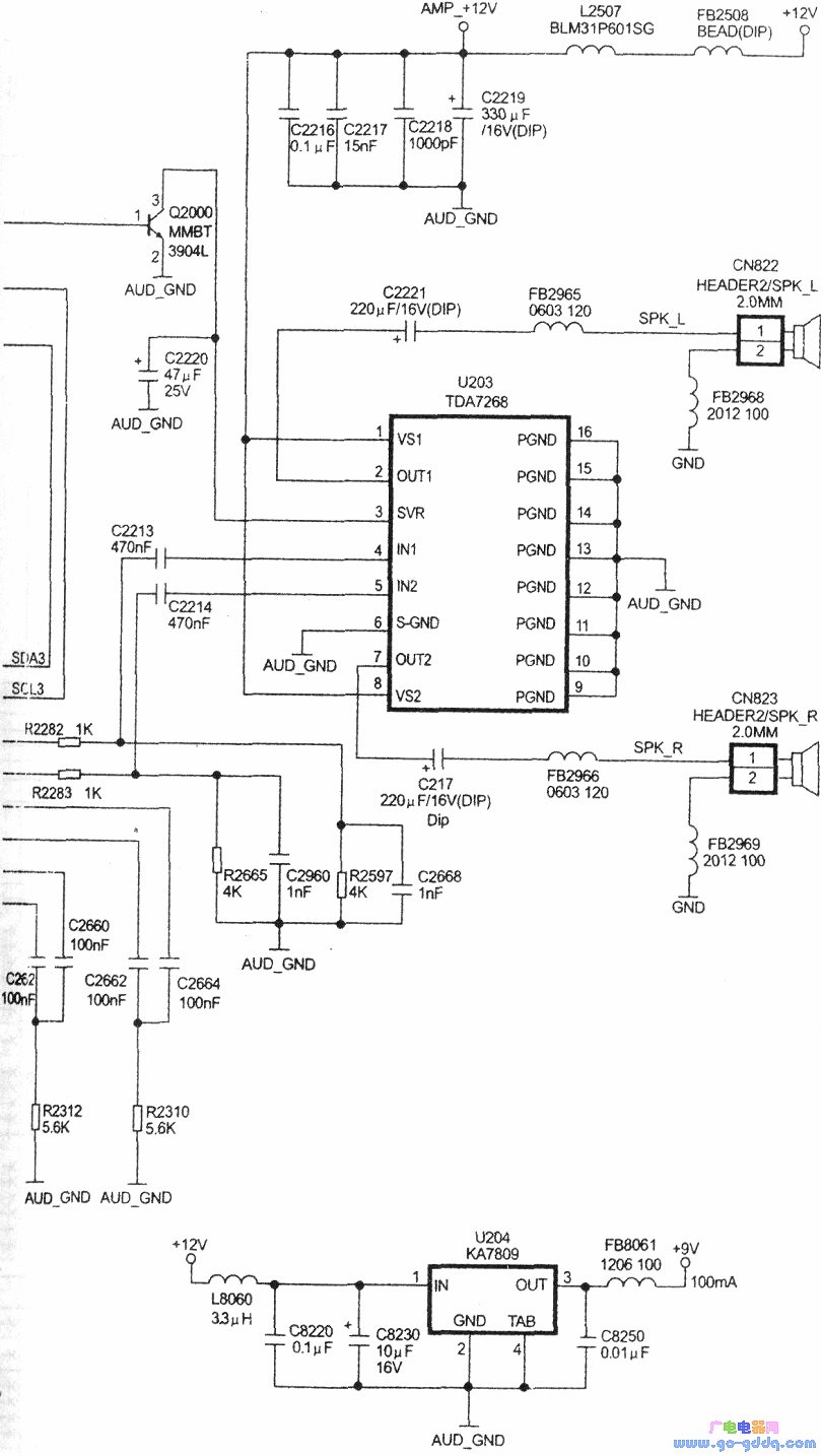
TDA7440D Sound Processing Circuit and TDA7268 Dual Audio Power Amplifier Output Circuit (b)
Key Features & Advantages
Why Choose a Stereo Amplifier?
stereo sound amplifier,sound amplifier,home audio amplifier,hi fi amp
Guangzhou Aiwo Audio Technology Co., LTD , https://www.aiwoaudio.com