Application of Global Shutter Pixel Technology on CMOS Image Sensors
Historically, global shutter pixel technology has been predominantly associated with CCD image sensors. However, as CMOS image sensors gained popularity due to their lower power consumption, higher integration, and cost-effectiveness, companies like ApTIna have been working to adapt global shutter technology for CMOS platforms. This shift is driven by the growing demand in machine vision, film production, industrial automation, automotive systems, and scanning applications that require high-quality imaging of fast-moving objects. Overcoming traditional challenges such as limited pixel size, reduced fill factor, and higher noise levels, the new global shutter technology on CMOS offers smaller pixels, improved light capture efficiency, better dynamic range, and reduced dark current, making it a strong alternative to traditional CCDs.
Rolling shutter technology, also known as focal-plane shutter, operates by sequentially exposing and reading out rows of pixels. A shutter pulse resets one row of pixels before it is read out, and the time between this reset and the readout determines the exposure duration. However, because each row is exposed at a slightly different time, rolling shutters can introduce distortion when capturing fast-moving subjects. This makes them unsuitable for applications like barcode scanning, machine vision, or automated inspection systems, where accurate and undistorted imaging is essential.
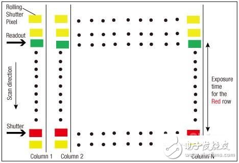
Figure 1: How the typical rolling shutter works
Many photographers and videographers have noticed that rolling shutters do not capture an entire frame at once. Instead, they scan the image line by line, either vertically or horizontally. While this allows for continuous photon collection and improved light sensitivity, it also leads to issues like motion distortion, smear, or partial exposure—especially under challenging lighting conditions or when filming fast-moving subjects. These drawbacks have led to ongoing research into how to transition from rolling to global shutters.
Early attempts to implement global shutters on CMOS sensors faced significant obstacles. Adding extra memory cells to enable simultaneous exposure across the entire sensor often reduced the active photosensitive area, which negatively impacted quantum efficiency. Additionally, factors such as semiconductor manufacturing limitations, application-specific needs, market trends, and cost constraints made it difficult to justify the development of global shutter CMOS sensors at the time. As a result, progress was slow, and the technology remained largely unfeasible for commercial use.
Yixing Guangming Special Ceramics Co.,Ltd , https://www.yxgmtc.com