Artificial Intelligence
Ultra-Low-Noise LDO Achieves 6
Abstract: This ultra-low-noise LDO combines low-noise components with filtering to achieve an output noise performance of 6nV /  at 1kHz.
Of the many low-dropout (LDO) regulators used to regulate voltage in electronic systems, some are specifically designed for low-noise operaTIon. The MAX8887 low-noise LDO, for example, achieves a noise voltage of only 42µVRMS over the 10Hz to 100kHz range. ApplicaTIons such as the ultra-low-noise oscillators required in instrumentaTIon, however, require even lower noise. To fulfill that requirement, Figure 1 shows a combinaTIon of low-noise components and filtering that achieves an output noise of only 6nV / at 1kHz.
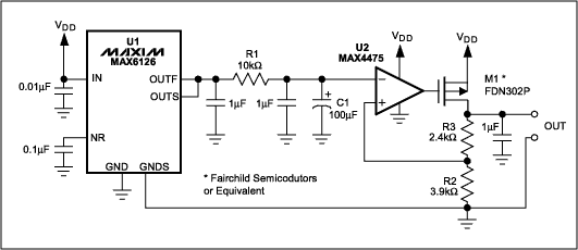
Figure 1. This ultra-low-noise LDO, the MAX6126, combines low-noise components with filtering to achieve an output noise floor of 6nV / .
In Figure 1, the MAX6126 (U1) is a voltage reference whose ultra-low output noise is further reduced by a lowpass filter (R1 and C1), which attenuates noise frequencies above its approximate 0.16Hz cutoff frequency. The filtered reference voltage is fed to the inverting terminal of error amplifier U2, which regulates the output voltage through a p-channel power FET (M1) and feedback resistors (R2 and R3). R2 and R3 determine the output voltage as follows:
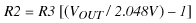
A simplified diagram for noise analysis (Figure 2) shows the reference noise filtered by lowpass filter R1-C1, which greatly attenuates the high-frequency noise (> f3dB). The op amp's noise current (specified at 0.5fA / ) is negligible with respect to its voltage noise. Because the reference noise is in series with the op-amp voltage noise, they add together. MOSFET noise is modeled at the input of M1.
Figure 2. Simplified diagram of the Figure 1 circuit, for noise analysis.
The noise at U2's inverting terminal equals the noise at its noninverting terminal:
where Vn_OUT is the LDO's output noise, Vn_REF is the reference noise, Vn_OPAMP is the op amp's input-referred noise, and H (f) is the transfer function for the R1-C1 lowpass filter.
If the noise frequency of interest is well above the filter's cutoff frequency, the reference noise is negligible, and the LDO's output noise is just the op-amp noise multiplied by the closed-loop gain. The MOSFET noise (Vn_FETs in Figure 2) is suppressed by the loop, and has no effect on the output noise. For frequencies within the loop bandwidth, the LDO also rejects ripple and noise voltages introduced by VDD.
A plot of noise density vs. frequency for the MAX6126 low-noise LDO (Figure 3) shows noise performance of about 6nV / at 1kHz. In comparison, typical low-noise LDOs have a much higher noise density—for example, the MAX8887 exhibits 500nV / vHz at 1kHz. Thus, the Figure 1 circuit shows a 38dB improvement over the MAX8887 low-noise LDO. The noise floor of the measuring instrument is also shown.
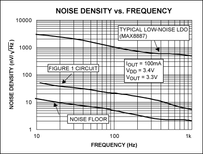
Figure 3. Noise density vs. frequency plot for the LDO circuit in Figure 1. Its noise performance is compared with that of the MAX8887, a typical low-noise LDO.
This design idea appeared in the June 23, 2005 issue of EDN.
at 1kHz. Of the many low-dropout (LDO) regulators used to regulate voltage in electronic systems, some are specifically designed for low-noise operaTIon. The MAX8887 low-noise LDO, for example, achieves a noise voltage of only 42µVRMS over the 10Hz to 100kHz range. ApplicaTIons such as the ultra-low-noise oscillators required in instrumentaTIon, however, require even lower noise. To fulfill that requirement, Figure 1 shows a combinaTIon of low-noise components and filtering that achieves an output noise of only 6nV /
at 1kHz. Figure 1. This ultra-low-noise LDO, the MAX6126, combines low-noise components with filtering to achieve an output noise floor of 6nV /
. In Figure 1, the MAX6126 (U1) is a voltage reference whose ultra-low output noise is further reduced by a lowpass filter (R1 and C1), which attenuates noise frequencies above its approximate 0.16Hz cutoff frequency. The filtered reference voltage is fed to the inverting terminal of error amplifier U2, which regulates the output voltage through a p-channel power FET (M1) and feedback resistors (R2 and R3). R2 and R3 determine the output voltage as follows:
A simplified diagram for noise analysis (Figure 2) shows the reference noise filtered by lowpass filter R1-C1, which greatly attenuates the high-frequency noise (> f3dB). The op amp's noise current (specified at 0.5fA /
) is negligible with respect to its voltage noise. Because the reference noise is in series with the op-amp voltage noise, they add together. MOSFET noise is modeled at the input of M1. Figure 2. Simplified diagram of the Figure 1 circuit, for noise analysis.
The noise at U2's inverting terminal equals the noise at its noninverting terminal:
where Vn_OUT is the LDO's output noise, Vn_REF is the reference noise, Vn_OPAMP is the op amp's input-referred noise, and H (f) is the transfer function for the R1-C1 lowpass filter.
If the noise frequency of interest is well above the filter's cutoff frequency, the reference noise is negligible, and the LDO's output noise is just the op-amp noise multiplied by the closed-loop gain. The MOSFET noise (Vn_FETs in Figure 2) is suppressed by the loop, and has no effect on the output noise. For frequencies within the loop bandwidth, the LDO also rejects ripple and noise voltages introduced by VDD.
A plot of noise density vs. frequency for the MAX6126 low-noise LDO (Figure 3) shows noise performance of about 6nV /
at 1kHz. In comparison, typical low-noise LDOs have a much higher noise density—for example, the MAX8887 exhibits 500nV / vHz at 1kHz. Thus, the Figure 1 circuit shows a 38dB improvement over the MAX8887 low-noise LDO. The noise floor of the measuring instrument is also shown. Figure 3. Noise density vs. frequency plot for the LDO circuit in Figure 1. Its noise performance is compared with that of the MAX8887, a typical low-noise LDO.
This design idea appeared in the June 23, 2005 issue of EDN.
Stellar provides industrial motherboards, Android motherboards, Windows motherboards, and LCD module kits according to the different needs of customers. LCD kit includes: LCD panel, AD board, inverter board and backlight cable, OSD button and cable, LVDS cable, touch screen, optical bonding, industrial keyboard, etc.
Indusrial Motherboard,Windows Motherboard,Android Mainboard,Pc Motherboard
Shenzhen Hengstar Technology Co., Ltd. , https://www.angeltondal.com